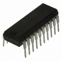
R5F211B4DD#ES Renesas Electronics America, R5F211B4DD#ES Datasheet - Page 31

R5F211B4DD#ES
Manufacturer Part Number
R5F211B4DD#ES
Description
MCU 3/5V 16K PB-FREE 20-SDIP ES
Manufacturer
Renesas Electronics America
Series
M16C™ M16C/R8C/Tiny/1Br
Datasheet
1.R5F211A2SPU0.pdf
(51 pages)
Specifications of R5F211B4DD#ES
Core Processor
R8C
Core Size
16-Bit
Speed
20MHz
Connectivity
I²C, SIO, SSU, UART/USART
Peripherals
LED, POR, Voltage Detect, WDT
Number Of I /o
13
Program Memory Size
16KB (16K x 8)
Program Memory Type
FLASH
Ram Size
1K x 8
Voltage - Supply (vcc/vdd)
2.7 V ~ 5.5 V
Data Converters
A/D 4x10b
Oscillator Type
Internal
Operating Temperature
-20°C ~ 85°C
Package / Case
20-DIP (0.300", 7.62mm)
For Use With
R0E521174CPE10 - EMULATOR COMPACT R8C/18/19/1
Lead Free Status / RoHS Status
Lead free / RoHS Compliant
Eeprom Size
-
Available stocks
Company
Part Number
Manufacturer
Quantity
Price
R8C/1A Group, R8C/1B Group
Rev.1.40
REJ03B0144-0140
Figure 5.3
Table 5.8
NOTES:
Table 5.9
NOTES:
V
t
V
t
t
t
t
w(Vpor2-Vdet1)
w(Vpor1-Vdet1)
w(Vpor1-Vdet1)
w(Vpor1-Vdet1)
w(Vpor1-Vdet1)
Internal reset signal
por2
por1
Symbol
1. This condition is not applicable when using with Vcc ≥ 1.0 V.
2. When turning power on after the time to hold the external power below effective voltage (V
3. t
Symbol
1. When not using voltage monitor 1, use with Vcc≥ 2.7 V.
2. t
5.9 Reset Circuit Electrical Characteristics (When Not Using Voltage Monitor 1 Reset).
w(por2)
w(por1)
NOTES:
Dec 08, 2006
(“L” valid)
1. Hold the voltage inside the MCU operation voltage range (Vccmin or above) within the sampling time.
2. The sampling clock can be selected. Refer to 7. Voltage Detection Circuit for details.
3. V
V
V
is the time to hold the external power below effective voltage (V
is the time to hold the external power below effective voltage (V
Power-on reset valid voltage
Supply voltage rising time when power-on reset is
deasserted
det1
por1
Power-on reset valid voltage
Supply voltage rising time when power-on reset is
deasserted
Supply voltage rising time when power-on reset is
deasserted
Supply voltage rising time when power-on reset is
deasserted
Supply voltage rising time when power-on reset is
deasserted
det1
Reset Circuit Electrical Characteristics (When Using Voltage Monitor 1 Reset)
Reset Circuit Electrical Characteristics
Reset Circuit Electrical Characteristics (When Not Using Voltage Monitor 1 Reset)
(3)
indicates the voltage detection level of the voltage detection 1 circuit. Refer to 7. Voltage Detection Circuit for details.
t
(1)
w(por1)
Page 29 of 45
Parameter
t
w(Vpor1–Vdet1)
Parameter
f
RING-S
1
× 32
Sampling time
-20°C ≤ Topr ≤ 85°C
-20°C ≤ Topr ≤ 85°C,
t
w(por2)
(1, 2)
≥ 0s
-20°C ≤ Topr ≤ 85°C
0°C ≤ Topr ≤ 85°C,
t
-20°C ≤ Topr < 0°C,
t
-20°C ≤ Topr < 0°C,
t
0°C ≤ Topr ≤ 85°C,
t
Condition
por2
por1
w(por1)
w(por1)
w(por1)
w(por1)
t
w(por2)
(3)
).
).
Condition
≥ 10 s
≥ 30 s
≥ 10 s
≥ 1 s
t
w(Vpor2–Vdet1)
(2)
(2)
(2)
(2)
V
Vccmin
por2
f
RING-S
por1
Min.
1
−
−
5. Electrical Characteristics
) exceeds10 s, refer to Table
Min.
−
−
−
−
−
Standard
× 32
Typ.
Standard
V
−
−
det1
Typ.
−
−
−
−
−
(3)
Max.
V
100
det1
Max.
100
100
0.1
0.5
1
Unit
ms
V
Unit
ms
ms
ms
ms
V


