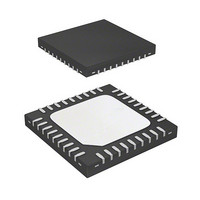
R5F213J6CNNP#U0 Renesas Electronics America, R5F213J6CNNP#U0 Datasheet - Page 543

R5F213J6CNNP#U0
Manufacturer Part Number
R5F213J6CNNP#U0
Description
MCU 1KB FLASH 32K ROM 36-QFN
Manufacturer
Renesas Electronics America
Series
R8C/3x/3JCr
Datasheet
1.R5F213J6CNNPU0.pdf
(750 pages)
Specifications of R5F213J6CNNP#U0
Core Processor
R8C
Core Size
16/32-Bit
Speed
20MHz
Connectivity
I²C, LIN, SIO, SSU, UART/USART
Peripherals
POR, PWM, Voltage Detect, WDT
Number Of I /o
31
Program Memory Size
32KB (32K x 8)
Program Memory Type
FLASH
Ram Size
2.5K x 8
Voltage - Supply (vcc/vdd)
1.8 V ~ 5.5 V
Data Converters
A/D 10x10b, D/A 2x8b
Oscillator Type
Internal
Operating Temperature
-20°C ~ 85°C
Package / Case
36-WQFN Exposed Pad, 36-HWQFN
Lead Free Status / RoHS Status
Lead free / RoHS Compliant
Eeprom Size
-
Available stocks
Company
Part Number
Manufacturer
Quantity
Price
- Current page: 543 of 750
- Download datasheet (8Mb)
R8C/3JC Group
REJ09B0602-0100 Rev.1.00
May 12, 2010
Figure 25.8
(1)
(2)
(3)
(4)
(5)
(6)
(7)
SSCRH register
SSCRH register
SSER register
Mode)
Sample Flowchart of Data Reception (MSS = 1) (Clock Synchronous Communication
Read receive data in SSRDR register
Read receive data in SSRDR register
Read ORER bit in SSSR register
Read ORER bit in SSSR register
Read RDRF bit in SSSR register
Dummy read of SSRDR register
Read RDRF in SSSR register
No
No
ORER = 1 ?
ORER = 1 ?
Initialization
RDRF = 1 ?
RDRF = 1 ?
received?
Last data
Start
End
RSSTP bit ← 1
RSSTP bit ← 0
RE bit ← 0
No
No
Yes
No
Yes
Yes
Yes
Yes
processing
Overrun
error
25. Synchronous Serial Communication Unit (SSU)
(3) If a receive error occurs, perform error
(6) processing after reading the ORER bit. Then set
(1) After setting each register in the synchronous serial
(2) Determine whether it is the last 1 byte of data to be
(4) Confirm that the RDRF bit is set to 1. If the RDRF
(5) Before the last 1 byte of data is received, set the
(7) Confirm that the RDRF bit is set to 1. When the
the ORER bit to 0. Transmission/reception cannot
be restarted while the ORER bit is set to 1.
communication unit register, a dummy read of the
SSRDR register is performed and the receive
operation is started.
received. If so, set to stop after the data is received.
bit is set to 1, read the receive data in the SSRDR
register. When the SSRDR register is read, the
RDRF bit is automatically set to 0.
RSSTP bit to 1 and stop after the data is
received.
receive operation is completed, set the RSSTP bit to
0 and the RE bit to 0 before reading the last 1 byte
of data. If the SSRDR register is read before setting
the RE bit to 0, the receive operation is restarted
again.
Page 512 of 715
Related parts for R5F213J6CNNP#U0
Image
Part Number
Description
Manufacturer
Datasheet
Request
R

Part Number:
Description:
KIT STARTER FOR M16C/29
Manufacturer:
Renesas Electronics America
Datasheet:

Part Number:
Description:
KIT STARTER FOR R8C/2D
Manufacturer:
Renesas Electronics America
Datasheet:

Part Number:
Description:
R0K33062P STARTER KIT
Manufacturer:
Renesas Electronics America
Datasheet:

Part Number:
Description:
KIT STARTER FOR R8C/23 E8A
Manufacturer:
Renesas Electronics America
Datasheet:

Part Number:
Description:
KIT STARTER FOR R8C/25
Manufacturer:
Renesas Electronics America
Datasheet:

Part Number:
Description:
KIT STARTER H8S2456 SHARPE DSPLY
Manufacturer:
Renesas Electronics America
Datasheet:

Part Number:
Description:
KIT STARTER FOR R8C38C
Manufacturer:
Renesas Electronics America
Datasheet:

Part Number:
Description:
KIT STARTER FOR R8C35C
Manufacturer:
Renesas Electronics America
Datasheet:

Part Number:
Description:
KIT STARTER FOR R8CL3AC+LCD APPS
Manufacturer:
Renesas Electronics America
Datasheet:

Part Number:
Description:
KIT STARTER FOR RX610
Manufacturer:
Renesas Electronics America
Datasheet:

Part Number:
Description:
KIT STARTER FOR R32C/118
Manufacturer:
Renesas Electronics America
Datasheet:

Part Number:
Description:
KIT DEV RSK-R8C/26-29
Manufacturer:
Renesas Electronics America
Datasheet:

Part Number:
Description:
KIT STARTER FOR SH7124
Manufacturer:
Renesas Electronics America
Datasheet:

Part Number:
Description:
KIT STARTER FOR H8SX/1622
Manufacturer:
Renesas Electronics America
Datasheet:

Part Number:
Description:
KIT DEV FOR SH7203
Manufacturer:
Renesas Electronics America
Datasheet:


