R5F213J6CNNP#U0 Renesas Electronics America, R5F213J6CNNP#U0 Datasheet - Page 189
R5F213J6CNNP#U0
Manufacturer Part Number
R5F213J6CNNP#U0
Description
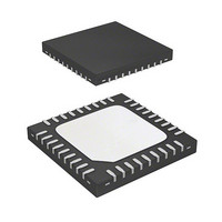
MCU 1KB FLASH 32K ROM 36-QFN
Manufacturer
Renesas Electronics America
Series
R8C/3x/3JCr
Datasheet
1.R5F213J6CNNPU0.pdf
(750 pages)
Specifications of R5F213J6CNNP#U0
Core Processor
R8C
Core Size
16/32-Bit
Speed
20MHz
Connectivity
I²C, LIN, SIO, SSU, UART/USART
Peripherals
POR, PWM, Voltage Detect, WDT
Number Of I /o
31
Program Memory Size
32KB (32K x 8)
Program Memory Type
FLASH
Ram Size
2.5K x 8
Voltage - Supply (vcc/vdd)
1.8 V ~ 5.5 V
Data Converters
A/D 10x10b, D/A 2x8b
Oscillator Type
Internal
Operating Temperature
-20°C ~ 85°C
Package / Case
36-WQFN Exposed Pad, 36-HWQFN
Lead Free Status / RoHS Status
Lead free / RoHS Compliant
Eeprom Size
-
Available stocks
Company
Part Number
Manufacturer
Quantity
Price


R8C/3JC Group
REJ09B0602-0100 Rev.1.00
May 12, 2010
Figure 11.9
Figure 11.10
11.4.5
INTi input
Sampling
timing
IR bit in
INTiIC register
The INTi input contains a digital filter. The sampling clock is selected using bits INTiF1 and INTiF0 in register
INTF. The INTi level is sampled every sampling clock cycle and if the sampled input level matches three times,
the IR bit in the INTiIC register is set to 1 (interrupt requested).
Figure 11.9 shows the INTi Input Filter Configuration. Figure 11.10 shows an Operating Example of INTi Input
Filter.
Note:
INTi Input Filter (i = 0 to 3)
Port direction
1. This is an operating example when bits INTiF1 to INTiF0 in register INTF are set to 01b, 10b, or 11b (digital filter
Note:
register
enabled).
i = 0 to 3
INTi Input Filter Configuration
Operating Example of INTi Input Filter
1. INT0: Port P4_5 direction register
INTi
INT1: Port P1_5 direction register when P1_5 pin used
INT2: Port P6_6 direction register when P6_6 pin used
INT3: Port P3_3 direction register when P3_3 pin used
(1)
INTiF0, INTiF1: Bits in register INTF
INTiEN, INTiPL: Bits in register INTEN
i = 0 to 3
f32
Port P1_7 direction register when P1_7 pin used
Port P2_0 direction register when P2_0 pin used
f1
f8
INTiF1 to INTiF0
= 01b
= 10b
= 11b
Sampling clock
Digital filter
(input level
matches
3 times)
Other than
INTiF1 to INTiF0
= 00b
INTiEN
= 00b
Both edges
detection
circuit
Set to 0 by a program.
INTiPL = 0
INTiPL = 1
INTi interrupt
Page 158 of 715
11. Interrupts
Related parts for R5F213J6CNNP#U0
Image
Part Number
Description
Manufacturer
Datasheet
Request
R

Part Number:
Description:
KIT STARTER FOR M16C/29
Manufacturer:
Renesas Electronics America
Datasheet:

Part Number:
Description:
KIT STARTER FOR R8C/2D
Manufacturer:
Renesas Electronics America
Datasheet:

Part Number:
Description:
R0K33062P STARTER KIT
Manufacturer:
Renesas Electronics America
Datasheet:

Part Number:
Description:
KIT STARTER FOR R8C/23 E8A
Manufacturer:
Renesas Electronics America
Datasheet:

Part Number:
Description:
KIT STARTER FOR R8C/25
Manufacturer:
Renesas Electronics America
Datasheet:

Part Number:
Description:
KIT STARTER H8S2456 SHARPE DSPLY
Manufacturer:
Renesas Electronics America
Datasheet:

Part Number:
Description:
KIT STARTER FOR R8C38C
Manufacturer:
Renesas Electronics America
Datasheet:

Part Number:
Description:
KIT STARTER FOR R8C35C
Manufacturer:
Renesas Electronics America
Datasheet:

Part Number:
Description:
KIT STARTER FOR R8CL3AC+LCD APPS
Manufacturer:
Renesas Electronics America
Datasheet:
Part Number:
Description:
KIT STARTER FOR RX610
Manufacturer:
Renesas Electronics America
Datasheet:

Part Number:
Description:
KIT STARTER FOR R32C/118
Manufacturer:
Renesas Electronics America
Datasheet:

Part Number:
Description:
KIT DEV RSK-R8C/26-29
Manufacturer:
Renesas Electronics America
Datasheet:

Part Number:
Description:
KIT STARTER FOR SH7124
Manufacturer:
Renesas Electronics America
Datasheet:

Part Number:
Description:
KIT STARTER FOR H8SX/1622
Manufacturer:
Renesas Electronics America
Datasheet:

Part Number:
Description:
KIT DEV FOR SH7203
Manufacturer:
Renesas Electronics America
Datasheet: