MC908AP32ACFBER Freescale Semiconductor, MC908AP32ACFBER Datasheet - Page 245
MC908AP32ACFBER
Manufacturer Part Number
MC908AP32ACFBER
Description
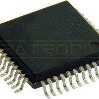
IC MCU 32K FLASH 8MHZ 44-QFP
Manufacturer
Freescale Semiconductor
Series
HC08r
Datasheet
1.MC908AP16ACFBER.pdf
(316 pages)
Specifications of MC908AP32ACFBER
Core Processor
HC08
Core Size
8-Bit
Speed
8MHz
Connectivity
I²C, IRSCI, SCI, SPI
Peripherals
LED, LVD, POR, PWM
Number Of I /o
32
Program Memory Size
32KB (32K x 8)
Program Memory Type
FLASH
Ram Size
2K x 8
Voltage - Supply (vcc/vdd)
4.5 V ~ 5.5 V
Data Converters
A/D 8x10b
Oscillator Type
Internal
Operating Temperature
-40°C ~ 85°C
Package / Case
44-QFP
Processor Series
HC08AP
Core
HC08
Data Bus Width
8 bit
Data Ram Size
2 KB
Interface Type
SCI, SPI
Maximum Clock Frequency
8 MHz
Number Of Programmable I/os
32
Number Of Timers
4
Maximum Operating Temperature
+ 85 C
Mounting Style
SMD/SMT
Development Tools By Supplier
FSICEBASE, DEMO908AP64E, M68CBL05CE
Minimum Operating Temperature
- 40 C
On-chip Adc
10 bit, 8 Channel
Lead Free Status / RoHS Status
Lead free / RoHS Compliant
Eeprom Size
-
Lead Free Status / Rohs Status
Details
Available stocks
Company
Part Number
Manufacturer
Quantity
Price
Company:

Part Number:
MC908AP32ACFBER
Manufacturer:
Freescale Semiconductor
Quantity:
10 000


Chapter 15
Analog-to-Digital Converter (ADC)
15.1 Introduction
This section describes the analog-to-digital converter (ADC). The ADC is a 8-channel 10-bit linear
successive approximation ADC.
15.2 Features
Features of the ADC module include:
Freescale Semiconductor
$0057
$0058
$0059
$005A
$005B
Addr.
•
•
•
•
•
•
•
•
•
Eight channels with multiplexed input
High impedance buffered input
Linear successive approximation with monotonicity
10-bit resolution
Single or continuous conversion
Auto-scan conversion on four channels
Conversion complete flag or conversion complete interrupt
Selectable ADC clock
Conversion result justification
–
–
–
–
ADC Data Register High 0
ADC Data Register Low 0
ADC Data Register Low 1
ADC Status and Control
8-bit truncated mode
Right justified mode
Left justified mode
Left justified sign mode
Register Name
ADC Clock Control
(ADICLK)
(ADSCR)
(ADRH0)
(ADRL0)
(ADRL1)
Register
Register
Reset:
Reset:
Reset:
Reset:
Reset:
Read:
Read:
Read:
Read:
Read:
Write:
Write:
Write:
Write:
Write:
Figure 15-1. ADC I/O Register Summary
MC68HC908AP A-Family Data Sheet, Rev. 3
COCO
ADIV2
Bit 7
AD9
ADx
ADx
R
R
R
0
0
0
0
0
ADIV1
AIEN
ADx
ADx
AD8
R
R
R
6
0
0
0
0
0
ADCO
ADIV0
ADx
ADx
AD7
R
R
R
5
0
0
0
0
0
ADICLK
ADCH4
ADx
ADx
AD6
R
R
R
4
1
0
0
0
0
MODE1
ADCH3
ADx
ADx
AD5
R
R
R
3
1
0
0
0
0
MODE0
ADCH2
ADx
ADx
AD4
R
R
R
2
1
1
0
0
0
ADCH1
ADx
ADx
AD3
R
R
R
1
1
0
0
0
0
0
ADCH0
Bit 0
AD2
ADx
ADx
R
R
R
R
1
0
0
0
0
0
245
Related parts for MC908AP32ACFBER
Image
Part Number
Description
Manufacturer
Datasheet
Request
R

Part Number:
Description:
Manufacturer:
Freescale Semiconductor, Inc
Datasheet:
Part Number:
Description:
Manufacturer:
Freescale Semiconductor, Inc
Datasheet:
Part Number:
Description:
Manufacturer:
Freescale Semiconductor, Inc
Datasheet:
Part Number:
Description:
Manufacturer:
Freescale Semiconductor, Inc
Datasheet:
Part Number:
Description:
Manufacturer:
Freescale Semiconductor, Inc
Datasheet:
Part Number:
Description:
Manufacturer:
Freescale Semiconductor, Inc
Datasheet:
Part Number:
Description:
Manufacturer:
Freescale Semiconductor, Inc
Datasheet:
Part Number:
Description:
Manufacturer:
Freescale Semiconductor, Inc
Datasheet:
Part Number:
Description:
Manufacturer:
Freescale Semiconductor, Inc
Datasheet:
Part Number:
Description:
Manufacturer:
Freescale Semiconductor, Inc
Datasheet:
Part Number:
Description:
Manufacturer:
Freescale Semiconductor, Inc
Datasheet:
Part Number:
Description:
Manufacturer:
Freescale Semiconductor, Inc
Datasheet:
Part Number:
Description:
Manufacturer:
Freescale Semiconductor, Inc
Datasheet:
Part Number:
Description:
Manufacturer:
Freescale Semiconductor, Inc
Datasheet:
Part Number:
Description:
Manufacturer:
Freescale Semiconductor, Inc
Datasheet: