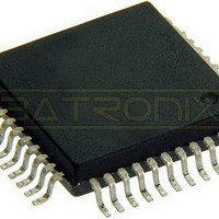
MC908AP32ACFBER Freescale Semiconductor, MC908AP32ACFBER Datasheet - Page 145

MC908AP32ACFBER
Manufacturer Part Number
MC908AP32ACFBER
Description
IC MCU 32K FLASH 8MHZ 44-QFP
Manufacturer
Freescale Semiconductor
Series
HC08r
Datasheet
1.MC908AP16ACFBER.pdf
(316 pages)
Specifications of MC908AP32ACFBER
Core Processor
HC08
Core Size
8-Bit
Speed
8MHz
Connectivity
I²C, IRSCI, SCI, SPI
Peripherals
LED, LVD, POR, PWM
Number Of I /o
32
Program Memory Size
32KB (32K x 8)
Program Memory Type
FLASH
Ram Size
2K x 8
Voltage - Supply (vcc/vdd)
4.5 V ~ 5.5 V
Data Converters
A/D 8x10b
Oscillator Type
Internal
Operating Temperature
-40°C ~ 85°C
Package / Case
44-QFP
Processor Series
HC08AP
Core
HC08
Data Bus Width
8 bit
Data Ram Size
2 KB
Interface Type
SCI, SPI
Maximum Clock Frequency
8 MHz
Number Of Programmable I/os
32
Number Of Timers
4
Maximum Operating Temperature
+ 85 C
Mounting Style
SMD/SMT
Development Tools By Supplier
FSICEBASE, DEMO908AP64E, M68CBL05CE
Minimum Operating Temperature
- 40 C
On-chip Adc
10 bit, 8 Channel
Lead Free Status / RoHS Status
Lead free / RoHS Compliant
Eeprom Size
-
Lead Free Status / Rohs Status
Details
Available stocks
Company
Part Number
Manufacturer
Quantity
Price
Company:
Part Number:
MC908AP32ACFBER
Manufacturer:
Freescale Semiconductor
Quantity:
10 000
- Current page: 145 of 316
- Download datasheet (2Mb)
9.9.5 TIM Channel Registers
These read/write registers contain the captured TIM counter value of the input capture function or the
output compare value of the output compare function. The state of the TIM channel registers after reset
is unknown.
In input capture mode (MSxB:MSxA = 0:0), reading the high byte of the TIM channel x registers (TCHxH)
inhibits input captures until the low byte (TCHxL) is read.
In output compare mode (MSxB:MSxA ≠ 0:0), writing to the high byte of the TIM channel x registers
(TCHxH) inhibits output compares until the low byte (TCHxL) is written.
Freescale Semiconductor
Address: T1CH0H, $0026 and T2CH0H, $0031
Address: T1CH0L, $0027 and T2CH0L $0032
Address: T1CH1H, $0029 and T2CH1H, $0034
CHxMAX
Reset:
Reset:
Reset:
Read:
Read:
Read:
Write:
Write:
Write:
TCHx
OVERFLOW
Bit 15
Bit 15
Bit 7
Bit 7
Bit 7
Bit 7
Figure 9-12. TIM Channel 0 Register High (TCH0H)
Figure 9-14. TIM Channel 1 Register High (TCH1H)
Figure 9-13. TIM Channel 0 Register Low (TCH0L)
COMPARE
PERIOD
OUTPUT
MC68HC908AP A-Family Data Sheet, Rev. 3
14
14
6
6
6
6
OVERFLOW
Figure 9-11. CHxMAX Latency
13
13
5
5
5
5
COMPARE
OUTPUT
Indeterminate after reset
Indeterminate after reset
Indeterminate after reset
OVERFLOW
12
12
4
4
4
4
COMPARE
OUTPUT
11
11
3
3
3
3
OVERFLOW
10
10
2
2
2
2
COMPARE
OUTPUT
OVERFLOW
1
9
1
1
1
9
Bit 0
Bit 8
Bit 0
Bit 0
Bit 0
Bit 8
I/O Registers
145
Related parts for MC908AP32ACFBER
Image
Part Number
Description
Manufacturer
Datasheet
Request
R
Part Number:
Description:
Manufacturer:
Freescale Semiconductor, Inc
Datasheet:
Part Number:
Description:
Manufacturer:
Freescale Semiconductor, Inc
Datasheet:
Part Number:
Description:
Manufacturer:
Freescale Semiconductor, Inc
Datasheet:
Part Number:
Description:
Manufacturer:
Freescale Semiconductor, Inc
Datasheet:
Part Number:
Description:
Manufacturer:
Freescale Semiconductor, Inc
Datasheet:
Part Number:
Description:
Manufacturer:
Freescale Semiconductor, Inc
Datasheet:
Part Number:
Description:
Manufacturer:
Freescale Semiconductor, Inc
Datasheet:
Part Number:
Description:
Manufacturer:
Freescale Semiconductor, Inc
Datasheet:
Part Number:
Description:
Manufacturer:
Freescale Semiconductor, Inc
Datasheet:
Part Number:
Description:
Manufacturer:
Freescale Semiconductor, Inc
Datasheet:
Part Number:
Description:
Manufacturer:
Freescale Semiconductor, Inc
Datasheet:
Part Number:
Description:
Manufacturer:
Freescale Semiconductor, Inc
Datasheet:
Part Number:
Description:
Manufacturer:
Freescale Semiconductor, Inc
Datasheet:
Part Number:
Description:
Manufacturer:
Freescale Semiconductor, Inc
Datasheet:
Part Number:
Description:
Manufacturer:
Freescale Semiconductor, Inc
Datasheet:


