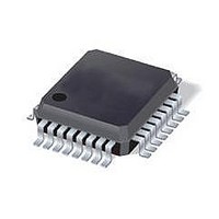
C8051F352-GQR Silicon Laboratories Inc, C8051F352-GQR Datasheet - Page 61

C8051F352-GQR
Manufacturer Part Number
C8051F352-GQR
Description
IC 8051 MCU 8K FLASH 32LQFP
Manufacturer
Silicon Laboratories Inc
Series
C8051F35xr
Specifications of C8051F352-GQR
Core Processor
8051
Core Size
8-Bit
Speed
50MHz
Connectivity
SMBus (2-Wire/I²C), SPI, UART/USART
Peripherals
POR, PWM, Temp Sensor, WDT
Number Of I /o
17
Program Memory Size
8KB (8K x 8)
Program Memory Type
FLASH
Ram Size
768 x 8
Voltage - Supply (vcc/vdd)
2.7 V ~ 3.6 V
Data Converters
A/D 8x16b; D/A 2x8b
Oscillator Type
Internal
Operating Temperature
-40°C ~ 85°C
Package / Case
32-LQFP
Core
8051
Processor Series
C8051F3x
Data Bus Width
8 bit
Maximum Clock Frequency
50 MHz
Data Ram Size
768 B
Data Rom Size
128 B
On-chip Adc
Yes
Number Of Programmable I/os
17
Number Of Timers
4 bit
Operating Supply Voltage
2.7 V to 3.6 V
Mounting Style
SMD/SMT
A/d Bit Size
16 bit
A/d Channels Available
8
Height
1.4 mm
Interface Type
I2C, SMBus, SPI, UART
Length
7 mm
Maximum Operating Temperature
+ 85 C
Minimum Operating Temperature
- 40 C
Supply Voltage (max)
3.6 V
Supply Voltage (min)
2.7 V
Width
7 mm
For Use With
336-1083 - DEV KIT FOR F350/351/352/353
Lead Free Status / RoHS Status
Lead free / RoHS Compliant
Eeprom Size
-
Lead Free Status / Rohs Status
Details
Available stocks
Company
Part Number
Manufacturer
Quantity
Price
Company:
Part Number:
C8051F352-GQR
Manufacturer:
Silicon Laboratories Inc
Quantity:
10 000
Company:
Part Number:
C8051F352-GQR..
Manufacturer:
SILICON
Quantity:
15 000
- Current page: 61 of 234
- Download datasheet (2Mb)
Table 5.3. ADC0 Electrical Characteristics
V
Decimation Ratio = 1920, –40 to +85 °C unless otherwise noted.
24-bit ADC (C8051F350/1)
Resolution
No Missing Codes
16-bit ADC (C8051F352/3)
Resolution
No Missing Codes
All Devices
Integral Nonlinearity
Offset Error (Calibrated)
Offset Drift vs. Temperature
Gain Error (Calibrated)
Gain Drift vs. Temperature
Modulator Clock (MDCLK)
Modulator Sampling Frequency
Output Word Rate
Analog Inputs
Analog Input Voltage Range
(AIN+ – AIN–)
Absolute Voltage on AIN+ or AIN–
pin with respect to AGND
Input Current
Input Impedance
Common Mode Rejection Ratio
Input Buffers
High Buffer Input Range with respect
to AGND
Low Buffer Input Range with respect
to AGND
Burnout Current Sources
Positive (AIN+) Channel Current
Negative (AIN–) Channel Current
DD
= AV+ = 3.0 V, VREF = 2.5 V External, PGA Gain = 1, MDCLK = 2.4576 MHz,
Parameter
PGA Gain = 1, 2, 4, or 8
PGA Gain = 1, 2, 4, or 8
PGA Gain = 1, Unipolar
PGA Gain = 1, Bipolar
PGA Gain = 64 or 128
PGA Gain = 64 or 128
Input Buffers OFF
Input Buffer OFF,
Input Buffer ON
PGA Gain = 16
PGA Gain = 32
PGA Gain = 16
PGA Gain = 32
VREF = 2.5 V
VREF = 2.5 V
Conditions
50/60 Hz
Gain = 1
Rev. 1.1
DC
–VREF
1.45
0.15
0.25
–0.9
Min
1.4
1.5
1.6
0.1
0.2
0.9
95
—
—
—
—
—
—
—
—
—
0
0
C8051F350/1/2/3
MDCLK/128
2.4576
±0.002
± 1.5
±0.5
Typ
100
110
±5
10
–2
—
—
—
—
—
—
—
—
—
—
—
—
—
7
2
24
24
16
16
AV+ – 0.15
AV+ – 0.25
AV+ – 1.45
AV+ – 0.1
AV+ – 0.2
AV+ – 1.4
AV+ – 1.5
AV+ – 1.6
+VREF
+VREF
1000
Max
–2.9
AV+
±15
2.9
30
—
—
—
—
—
—
—
—
Units
ppm/
MHz
ppm
ppm
bits
bits
bits
bits
nV/
sps
MΩ
FS
µA
µA
°C
°C
Hz
nA
dB
dB
%
V
V
V
V
V
V
V
V
V
V
61
Related parts for C8051F352-GQR
Image
Part Number
Description
Manufacturer
Datasheet
Request
R
Part Number:
Description:
SMD/C°/SINGLE-ENDED OUTPUT SILICON OSCILLATOR
Manufacturer:
Silicon Laboratories Inc
Part Number:
Description:
Manufacturer:
Silicon Laboratories Inc
Datasheet:
Part Number:
Description:
N/A N/A/SI4010 AES KEYFOB DEMO WITH LCD RX
Manufacturer:
Silicon Laboratories Inc
Datasheet:
Part Number:
Description:
N/A N/A/SI4010 SIMPLIFIED KEY FOB DEMO WITH LED RX
Manufacturer:
Silicon Laboratories Inc
Datasheet:
Part Number:
Description:
N/A/-40 TO 85 OC/EZLINK MODULE; F930/4432 HIGH BAND (REV E/B1)
Manufacturer:
Silicon Laboratories Inc
Part Number:
Description:
EZLink Module; F930/4432 Low Band (rev e/B1)
Manufacturer:
Silicon Laboratories Inc
Part Number:
Description:
I°/4460 10 DBM RADIO TEST CARD 434 MHZ
Manufacturer:
Silicon Laboratories Inc
Part Number:
Description:
I°/4461 14 DBM RADIO TEST CARD 868 MHZ
Manufacturer:
Silicon Laboratories Inc
Part Number:
Description:
I°/4463 20 DBM RFSWITCH RADIO TEST CARD 460 MHZ
Manufacturer:
Silicon Laboratories Inc
Part Number:
Description:
I°/4463 20 DBM RADIO TEST CARD 868 MHZ
Manufacturer:
Silicon Laboratories Inc
Part Number:
Description:
I°/4463 27 DBM RADIO TEST CARD 868 MHZ
Manufacturer:
Silicon Laboratories Inc
Part Number:
Description:
I°/4463 SKYWORKS 30 DBM RADIO TEST CARD 915 MHZ
Manufacturer:
Silicon Laboratories Inc
Part Number:
Description:
N/A N/A/-40 TO 85 OC/4463 RFMD 30 DBM RADIO TEST CARD 915 MHZ
Manufacturer:
Silicon Laboratories Inc
Part Number:
Description:
I°/4463 20 DBM RADIO TEST CARD 169 MHZ
Manufacturer:
Silicon Laboratories Inc


