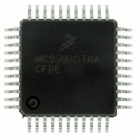
MC9S08GT8ACFBE Freescale Semiconductor, MC9S08GT8ACFBE Datasheet - Page 86

MC9S08GT8ACFBE
Manufacturer Part Number
MC9S08GT8ACFBE
Description
IC MCU 8K FLASH 1K RAM 44-QFP
Manufacturer
Freescale Semiconductor
Series
HCS08r
Datasheet
1.MC9S08GT8ACFBER.pdf
(300 pages)
Specifications of MC9S08GT8ACFBE
Core Processor
HCS08
Core Size
8-Bit
Speed
40MHz
Connectivity
I²C, SCI, SPI
Peripherals
LVD, POR, PWM, WDT
Number Of I /o
36
Program Memory Size
8KB (8K x 8)
Program Memory Type
FLASH
Ram Size
1K x 8
Voltage - Supply (vcc/vdd)
1.8 V ~ 3.6 V
Data Converters
A/D 8x10b
Oscillator Type
Internal
Operating Temperature
-40°C ~ 85°C
Package / Case
44-QFP
Processor Series
S08GT
Core
HCS08
Data Bus Width
8 bit
Data Ram Size
1 KB
Interface Type
I2C/SCI/SPI
Maximum Clock Frequency
40 MHz
Number Of Programmable I/os
36
Operating Supply Voltage
3.6 V
Maximum Operating Temperature
+ 85 C
Mounting Style
SMD/SMT
3rd Party Development Tools
EWS08
Development Tools By Supplier
M68EVB908GB60E, M68DEMO908GB60E
Minimum Operating Temperature
- 40 C
On-chip Adc
8-ch x 10-bit
For Use With
M68DEMO908GB60E - BOARD DEMO MC9S08GB60M68EVB908GB60E - BOARD EVAL FOR MC9S08GB60
Lead Free Status / RoHS Status
Lead free / RoHS Compliant
Eeprom Size
-
Lead Free Status / Rohs Status
Lead free / RoHS Compliant
Available stocks
Company
Part Number
Manufacturer
Quantity
Price
Company:
Part Number:
MC9S08GT8ACFBE
Manufacturer:
FREESCALE
Quantity:
1 600
Company:
Part Number:
MC9S08GT8ACFBE
Manufacturer:
Freescale Semiconductor
Quantity:
10 000
Company:
Part Number:
MC9S08GT8ACFBER
Manufacturer:
Freescale Semiconductor
Quantity:
10 000
- Current page: 86 of 300
- Download datasheet (2Mb)
Parallel Input/Output
6.4
Depending on the stop mode, I/O functions differently as the result of executing a STOP instruction. An
explanation of I/O behavior for the various stop modes follows:
6.5
This section provides information about all registers and control bits associated with the parallel I/O ports.
Refer to tables in
This section refers to registers and control bits only by their names. A Freescale-provided equate or header
file normally is used to translate these names into the appropriate absolute addresses.
6.5.1
Port A includes eight pins shared between general-purpose I/O and the KBI module. Port A pins used as
general-purpose I/O pins are controlled by the port A data (PTAD), data direction (PTADD), pullup enable
(PTAPE), and slew rate control (PTASE) registers.
If the KBI takes control of a port A pin, the corresponding PTASE bit is ignored since the pin functions as
an input. As long as PTADD is 0, the PTAPE controls the pullup enable for the KBI function. Reads of
PTAD will return the logic value of the corresponding pin, provided PTADD is 0.
86
•
•
•
When the MCU enters stop1 mode, all internal registers including general-purpose I/O control and
data registers are powered down. All of the general-purpose I/O pins assume their reset state:
output buffers and pullups turned off. Upon exit from stop1, all I/O must be initialized as if the
MCU had been reset.
When the MCU enters stop2 mode, the internal registers are powered down as in stop1 but the I/O
pin states are latched and held. For example, a port pin that is an output driving low continues to
function as an output driving low even though its associated data direction and output data registers
are powered down internally. Upon exit from stop2, the pins continue to hold their states until a 1
is written to the PPDACK bit. To avoid discontinuity in the pin state following exit from stop2, the
user must restore the port control and data registers to the values they held before entering stop2.
These values can be stored in RAM before entering stop2 because the RAM is maintained during
stop2.
In stop3 mode, all I/O is maintained because internal logic circuity stays powered up. Upon
recovery, normal I/O function is available to the user.
Stop Modes
Register Definition
Port A Registers (PTAD, PTAPE, PTASE, and PTADD)
Chapter 4,
“Memory,” for the absolute address assignments for all parallel I/O registers.
MC9S08GT16A/GT8A Data Sheet, Rev. 1
Freescale Semiconductor
Related parts for MC9S08GT8ACFBE
Image
Part Number
Description
Manufacturer
Datasheet
Request
R
Part Number:
Description:
Manufacturer:
Freescale Semiconductor, Inc
Datasheet:
Part Number:
Description:
Manufacturer:
Freescale Semiconductor, Inc
Datasheet:
Part Number:
Description:
Manufacturer:
Freescale Semiconductor, Inc
Datasheet:
Part Number:
Description:
Manufacturer:
Freescale Semiconductor, Inc
Datasheet:
Part Number:
Description:
Manufacturer:
Freescale Semiconductor, Inc
Datasheet:
Part Number:
Description:
Manufacturer:
Freescale Semiconductor, Inc
Datasheet:
Part Number:
Description:
Manufacturer:
Freescale Semiconductor, Inc
Datasheet:
Part Number:
Description:
Manufacturer:
Freescale Semiconductor, Inc
Datasheet:
Part Number:
Description:
Manufacturer:
Freescale Semiconductor, Inc
Datasheet:
Part Number:
Description:
Manufacturer:
Freescale Semiconductor, Inc
Datasheet:
Part Number:
Description:
Manufacturer:
Freescale Semiconductor, Inc
Datasheet:
Part Number:
Description:
Manufacturer:
Freescale Semiconductor, Inc
Datasheet:
Part Number:
Description:
Manufacturer:
Freescale Semiconductor, Inc
Datasheet:
Part Number:
Description:
Manufacturer:
Freescale Semiconductor, Inc
Datasheet:
Part Number:
Description:
Manufacturer:
Freescale Semiconductor, Inc
Datasheet:


