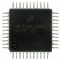
MC9S08GT8ACFBE Freescale Semiconductor, MC9S08GT8ACFBE Datasheet - Page 79

MC9S08GT8ACFBE
Manufacturer Part Number
MC9S08GT8ACFBE
Description
IC MCU 8K FLASH 1K RAM 44-QFP
Manufacturer
Freescale Semiconductor
Series
HCS08r
Datasheet
1.MC9S08GT8ACFBER.pdf
(300 pages)
Specifications of MC9S08GT8ACFBE
Core Processor
HCS08
Core Size
8-Bit
Speed
40MHz
Connectivity
I²C, SCI, SPI
Peripherals
LVD, POR, PWM, WDT
Number Of I /o
36
Program Memory Size
8KB (8K x 8)
Program Memory Type
FLASH
Ram Size
1K x 8
Voltage - Supply (vcc/vdd)
1.8 V ~ 3.6 V
Data Converters
A/D 8x10b
Oscillator Type
Internal
Operating Temperature
-40°C ~ 85°C
Package / Case
44-QFP
Processor Series
S08GT
Core
HCS08
Data Bus Width
8 bit
Data Ram Size
1 KB
Interface Type
I2C/SCI/SPI
Maximum Clock Frequency
40 MHz
Number Of Programmable I/os
36
Operating Supply Voltage
3.6 V
Maximum Operating Temperature
+ 85 C
Mounting Style
SMD/SMT
3rd Party Development Tools
EWS08
Development Tools By Supplier
M68EVB908GB60E, M68DEMO908GB60E
Minimum Operating Temperature
- 40 C
On-chip Adc
8-ch x 10-bit
For Use With
M68DEMO908GB60E - BOARD DEMO MC9S08GB60M68EVB908GB60E - BOARD EVAL FOR MC9S08GB60
Lead Free Status / RoHS Status
Lead free / RoHS Compliant
Eeprom Size
-
Lead Free Status / Rohs Status
Lead free / RoHS Compliant
Available stocks
Company
Part Number
Manufacturer
Quantity
Price
Company:
Part Number:
MC9S08GT8ACFBE
Manufacturer:
FREESCALE
Quantity:
1 600
Company:
Part Number:
MC9S08GT8ACFBE
Manufacturer:
Freescale Semiconductor
Quantity:
10 000
Company:
Part Number:
MC9S08GT8ACFBER
Manufacturer:
Freescale Semiconductor
Quantity:
10 000
- Current page: 79 of 300
- Download datasheet (2Mb)
Chapter 6
Parallel Input/Output
6.1
This section explains software controls related to parallel input/output (I/O). The MC9S08GT16A/GT8A
has six I/O ports which include a total of up to 39 general-purpose I/O pins (one pin, PTG0, is output only).
See
pins.
Many of these pins are shared with on-chip peripherals such as timer systems, external interrupts, or
keyboard interrupts. When these other modules are not controlling the port pins, they revert to
general-purpose I/O control. For each I/O pin, a port data bit provides access to input (read) and output
(write) data, a data direction bit controls the direction of the pin, and a pullup enable bit enables an internal
pullup device (provided the pin is configured as an input), and a slew rate control bit controls the rise and
fall times of the pins.
Pins that are not used in the application must be terminated. This prevents excess current caused by floating
inputs and enhances immunity during noise or transient events. Termination methods include:
Never connect unused pins to V
6.1.1
Parallel I/O features, depending on package choice, include:
Freescale Semiconductor
•
•
•
•
•
•
•
•
Chapter 2, “Pins and
Configuring unused pins as outputs driving high or low
Configuring unused pins as inputs and using internal or external pullups
A total of 39 general-purpose I/O pins in six ports (PTG0 is output only)
High-current drivers on port C pins
Hysteresis input buffers
Software-controlled pullups on each input pin
Software-controlled slew rate output buffers
Eight port A pins shared with KBI
Introduction
Features
Not all general-purpose I/O pins are available on all packages. To avoid
extra current drain from floating input pins, the user’s reset initialization
routine in the application program should either enable on-chip pullup
devices or change the direction of unconnected pins to outputs so the pins
do not float.
Connections,” for more information about the logic and hardware aspects of these
DD
MC9S08GT16A/GT8A Data Sheet, Rev. 1
or V
SS
.
NOTE
79
Related parts for MC9S08GT8ACFBE
Image
Part Number
Description
Manufacturer
Datasheet
Request
R
Part Number:
Description:
Manufacturer:
Freescale Semiconductor, Inc
Datasheet:
Part Number:
Description:
Manufacturer:
Freescale Semiconductor, Inc
Datasheet:
Part Number:
Description:
Manufacturer:
Freescale Semiconductor, Inc
Datasheet:
Part Number:
Description:
Manufacturer:
Freescale Semiconductor, Inc
Datasheet:
Part Number:
Description:
Manufacturer:
Freescale Semiconductor, Inc
Datasheet:
Part Number:
Description:
Manufacturer:
Freescale Semiconductor, Inc
Datasheet:
Part Number:
Description:
Manufacturer:
Freescale Semiconductor, Inc
Datasheet:
Part Number:
Description:
Manufacturer:
Freescale Semiconductor, Inc
Datasheet:
Part Number:
Description:
Manufacturer:
Freescale Semiconductor, Inc
Datasheet:
Part Number:
Description:
Manufacturer:
Freescale Semiconductor, Inc
Datasheet:
Part Number:
Description:
Manufacturer:
Freescale Semiconductor, Inc
Datasheet:
Part Number:
Description:
Manufacturer:
Freescale Semiconductor, Inc
Datasheet:
Part Number:
Description:
Manufacturer:
Freescale Semiconductor, Inc
Datasheet:
Part Number:
Description:
Manufacturer:
Freescale Semiconductor, Inc
Datasheet:
Part Number:
Description:
Manufacturer:
Freescale Semiconductor, Inc
Datasheet:


