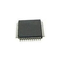
MC9S08JM8CLD Freescale Semiconductor, MC9S08JM8CLD Datasheet - Page 187

MC9S08JM8CLD
Manufacturer Part Number
MC9S08JM8CLD
Description
MCU 8BIT 8K FLASH 44-LQFP
Manufacturer
Freescale Semiconductor
Series
HCS08r
Datasheet
1.DEMO9S08JM16.pdf
(386 pages)
Specifications of MC9S08JM8CLD
Core Processor
HCS08
Core Size
8-Bit
Speed
48MHz
Connectivity
I²C, LIN, SCI, SPI, USB
Peripherals
LVD, POR, PWM, WDT
Number Of I /o
33
Program Memory Size
8KB (8K x 8)
Program Memory Type
FLASH
Ram Size
1K x 8
Voltage - Supply (vcc/vdd)
2.7 V ~ 5.5 V
Data Converters
A/D 8x12b
Oscillator Type
External
Operating Temperature
-40°C ~ 85°C
Package / Case
44-LQFP
Processor Series
S08JM
Core
HCS08
Data Bus Width
8 bit
Data Ram Size
1 KB
Interface Type
I2C, SPI
Maximum Clock Frequency
48 MHz
Number Of Programmable I/os
37
Number Of Timers
2
Operating Supply Voltage
2.7 V to 5.5 V
Maximum Operating Temperature
+ 85 C
Mounting Style
SMD/SMT
3rd Party Development Tools
EWS08
Development Tools By Supplier
DEMOJM, DEMOJMSKT, DEMOFLEXISJMSD, DEMO9S08JM16
Minimum Operating Temperature
- 40 C
On-chip Adc
12 bit, 8 Channel
Controller Family/series
HCS08
No. Of I/o's
33
Ram Memory Size
1KB
Cpu Speed
48MHz
No. Of Timers
2
Digital Ic Case Style
LQFP
Rohs Compliant
Yes
Lead Free Status / RoHS Status
Lead free / RoHS Compliant
Eeprom Size
-
Lead Free Status / Rohs Status
Lead free / RoHS Compliant
Available stocks
Company
Part Number
Manufacturer
Quantity
Price
Company:
Part Number:
MC9S08JM8CLD
Manufacturer:
Freescale Semiconductor
Quantity:
10 000
- Current page: 187 of 386
- Download datasheet (8Mb)
Freescale Semiconductor
Field
CME
VDIV
3:0
5
Clock Monitor Enable — Determines if a reset request is made following a loss of external clock indication. The
CME bit must only be set to a logic 1 when either the MCG is in an operational mode that uses the external clock
(FEE, FBE, PEE, PBE, or BLPE) or the external reference is enabled (ERCLKEN=1 in the MCGC2 register).
Whenever the CME bit is set to a logic 1, the value of the RANGE bit in the MCGC2 register must not be changed.
0 Clock monitor is disabled.
1 Generate a reset request on loss of external clock.
VCO Divider — Selects the amount to divide down the VCO output of PLL. The VDIV bits establish the
multiplication factor (M) applied to the reference clock frequency.
0000 Encoding 0 — Reserved.
0001 Encoding 1 — Multiply by 4.
0010 Encoding 2 — Multiply by 8.
0011 Encoding 3 — Multiply by 12.
0100 Encoding 4 — Multiply by 16.
0101 Encoding 5 — Multiply by 20.
0110 Encoding 6 — Multiply by 24.
0111 Encoding 7 — Multiply by 28.
1000 Encoding 8 — Multiply by 32.
1001 Encoding 9 — Multiply by 36.
1010 Encoding 10 — Multiply by 40.
1011 Encoding 11 — Reserved (default to M=40).
11xx Encoding 12-15 — Reserved (default to M=40).
Table 12-5. MCG PLL Register Field Descriptions (continued)
MC9S08JM16 Series Data Sheet, Rev. 2
Description
Multi-Purpose Clock Generator (S08MCGV1)
187
Related parts for MC9S08JM8CLD
Image
Part Number
Description
Manufacturer
Datasheet
Request
R
Part Number:
Description:
Manufacturer:
Freescale Semiconductor, Inc
Datasheet:
Part Number:
Description:
Manufacturer:
Freescale Semiconductor, Inc
Datasheet:
Part Number:
Description:
Manufacturer:
Freescale Semiconductor, Inc
Datasheet:
Part Number:
Description:
Manufacturer:
Freescale Semiconductor, Inc
Datasheet:
Part Number:
Description:
Manufacturer:
Freescale Semiconductor, Inc
Datasheet:
Part Number:
Description:
Manufacturer:
Freescale Semiconductor, Inc
Datasheet:
Part Number:
Description:
Manufacturer:
Freescale Semiconductor, Inc
Datasheet:
Part Number:
Description:
Manufacturer:
Freescale Semiconductor, Inc
Datasheet:
Part Number:
Description:
Manufacturer:
Freescale Semiconductor, Inc
Datasheet:
Part Number:
Description:
Manufacturer:
Freescale Semiconductor, Inc
Datasheet:
Part Number:
Description:
Manufacturer:
Freescale Semiconductor, Inc
Datasheet:
Part Number:
Description:
Manufacturer:
Freescale Semiconductor, Inc
Datasheet:
Part Number:
Description:
Manufacturer:
Freescale Semiconductor, Inc
Datasheet:
Part Number:
Description:
Manufacturer:
Freescale Semiconductor, Inc
Datasheet:
Part Number:
Description:
Manufacturer:
Freescale Semiconductor, Inc
Datasheet:


