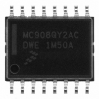
MC908QY2ACDWE Freescale Semiconductor, MC908QY2ACDWE Datasheet - Page 148

MC908QY2ACDWE
Manufacturer Part Number
MC908QY2ACDWE
Description
IC MCU 8BIT 1.5K FLASH 16SOIC
Manufacturer
Freescale Semiconductor
Series
HC08r
Datasheet
1.MC908QT1ACDWE.pdf
(200 pages)
Specifications of MC908QY2ACDWE
Core Processor
HC08
Core Size
8-Bit
Speed
8MHz
Peripherals
LVD, POR, PWM
Number Of I /o
13
Program Memory Size
1.5KB (1.5K x 8)
Program Memory Type
FLASH
Ram Size
128 x 8
Voltage - Supply (vcc/vdd)
2.7 V ~ 5.5 V
Data Converters
A/D 6x10b
Oscillator Type
Internal
Operating Temperature
-40°C ~ 85°C
Package / Case
16-SOIC (0.300", 7.5mm Width)
Processor Series
HC08QY
Core
HC08
Data Bus Width
8 bit
Data Ram Size
128 B
Maximum Clock Frequency
8 MHz
Number Of Programmable I/os
13
Number Of Timers
2
Maximum Operating Temperature
+ 85 C
Mounting Style
SMD/SMT
Development Tools By Supplier
FSICEBASE, M68CBL05AE, DEMO908QB8, DEMO908QC16
Minimum Operating Temperature
- 40 C
On-chip Adc
10 bit, 6 Channel
Lead Free Status / RoHS Status
Lead free / RoHS Compliant
Eeprom Size
-
Connectivity
-
Lead Free Status / Rohs Status
Details
Available stocks
Company
Part Number
Manufacturer
Quantity
Price
Company:
Part Number:
MC908QY2ACDWE
Manufacturer:
MITSUBISHI
Quantity:
210
Part Number:
MC908QY2ACDWE
Manufacturer:
FREESCALE
Quantity:
20 000
Development Support
15.3.1.1 Normal Monitor Mode
RST and OSC1 functions will be active on the PTA3 and PTA5 pins respectively as long as V
applied to the IRQ pin. If the IRQ pin is lowered (no longer V
monitor mode, but the pin functions will be determined by the settings in the configuration registers (see
Chapter 5 Configuration Register
BIL instructions will read the IRQ pin state only if IRQEN is set in the CONFIG2 register.
If monitor mode was entered with V
IRQ.
15.3.1.2 Forced Monitor Mode
If entering monitor mode without high voltage on IRQ, then startup port pin requirements and conditions,
(PTA1/PTA4) are not in effect. This is to reduce circuit requirements when performing in-circuit
programming.
148
Function
[Pin No.]
MON08
Monitor
Monitor
Normal
Forced
Mode
1. PTA0 must have a pullup resistor to V
2. Communication speed in the table is an example to obtain a baud rate of 9600. Baud rate using external oscillator is bus
3. External clock is a 9.8304 MHz oscillator on OSC1.
4. Lowering V
5. X = don’t care
6. MON08 pin refers to P&E Microcomputer Systems’ MON08-Cyclone 2 by 8-pin connector.
User
frequency / 256 and baud rate using internal oscillator is bus frequency / 335.
(PTA2)
V
V
IRQ
V
V
[6]
TST
TST
X
DD
SS
TST
once monitor mode is entered allows the clock source to be controlled by the OSCSC register.
(PTA3)
RST
RST
V
[4]
X
X
X
DD
Table 15-1. Monitor Mode Signal Requirements and Options
Vector
$FFFF
(blank)
$FFFF
(blank)
$FFFF
Reset
Not
—
X
MC68HC908QYA/QTA Family Data Sheet, Rev. 3
Communi-
cation
Serial
PTA0
COM
(CONFIG)) when V
[8]
DD
1
1
1
X
TST
OSC1
V
in monitor mode.
NC
NC
NC
NC
NC
NC
DD
on IRQ, then the COP is disabled as long as V
MOD0
PTA1 PTA4
[12]
Selection
11
13
15
X
X
X
1
1
3
5
7
9
Mode
MOD1
[10]
10
12
14
16
X
X
X
0
2
4
6
8
TST
Disabled
Disabled
Disabled
GND
RST
IRQ
PTA0
PTA4
PTA1
NC
NC
Enabled
COP
—
was lowered. With V
TST
External
) then the chip will still be operating in
9.8304
9.8304
Clock
OSC1
MHz
MHz
[13]
X
X
Communication
Frequency
(Trimmed)
Speed
3.2 MHz
2.4576
2.4576
MHz
MHz
Bus
—
X
TST
lowered, the BIH and
Freescale Semiconductor
Baud
Rate
9600
9600
9600
—
X
TST
Provide external
clock at OSC1.
Provide external
clock at OSC1.
Internal clock is
active.
is applied to
Comments
TST
is


