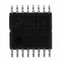
MC908QY1ACDTE Freescale Semiconductor, MC908QY1ACDTE Datasheet - Page 107

MC908QY1ACDTE
Manufacturer Part Number
MC908QY1ACDTE
Description
IC MCU 8BIT 1.5K FLASH 16TSSOP
Manufacturer
Freescale Semiconductor
Series
HC08r
Datasheet
1.MC908QT1ACDWE.pdf
(200 pages)
Specifications of MC908QY1ACDTE
Core Processor
HC08
Core Size
8-Bit
Speed
8MHz
Peripherals
LVD, POR, PWM
Number Of I /o
13
Program Memory Size
1.5KB (1.5K x 8)
Program Memory Type
FLASH
Ram Size
128 x 8
Voltage - Supply (vcc/vdd)
2.7 V ~ 5.5 V
Oscillator Type
Internal
Operating Temperature
-40°C ~ 85°C
Package / Case
16-TSSOP
Processor Series
HC08QY
Core
HC08
Data Bus Width
8 bit
Data Ram Size
128 B
Maximum Clock Frequency
8 MHz
Number Of Programmable I/os
13
Number Of Timers
2
Maximum Operating Temperature
+ 85 C
Mounting Style
SMD/SMT
Development Tools By Supplier
FSICEBASE, M68CBL05AE, DEMO908QB8, DEMO908QC16
Minimum Operating Temperature
- 40 C
Lead Free Status / RoHS Status
Lead free / RoHS Compliant
Eeprom Size
-
Data Converters
-
Connectivity
-
Lead Free Status / Rohs Status
Details
- Current page: 107 of 200
- Download datasheet (2Mb)
12.4.2 Data Direction Register B
Data direction register B (DDRB) determines whether each port B pin is an input or an output. Writing a 1
to a DDRB bit enables the output buffer for the corresponding port B pin; a 0 disables the output buffer.
DDRB[7:0] — Data Direction Register B Bits
When DDRBx is a 1, reading PTB reads the PTBx data latch. When DDRBx is a 0, reading PTB reads
the logic level on the PTBx pin. The data latch can always be written, regardless of the state of its data
direction bit.
Freescale Semiconductor
These read/write bits control port B data direction. Reset clears DDRB[7:0], configuring all port B pins
as inputs.
1 = Corresponding port B pin configured as output
0 = Corresponding port B pin configured as input
Reset:
Read:
Write:
Avoid glitches on port B pins by writing to the port B data register before
changing data direction register B bits from 0 to 1.
port B I/O logic.
DDRB7
READ DDRB
WRITE DDRB
WRITE PTB
READ PTB
Bit 7
0
Figure 12-6. Data Direction Register B (DDRB)
DDRB6
MC68HC908QYA/QTA Family Data Sheet, Rev. 3
6
0
RESET
Figure 12-7. Port B I/O Circuit
DDRB5
5
0
DDRB4
NOTE
DDRBx
4
0
PTBx
DDRB3
3
0
Figure 12-7
DDRB2
2
0
PTBPUEx
DDRB1
1
0
shows the
DDRB0
PULLUP
Bit 0
0
PTBx
Port B
107
Related parts for MC908QY1ACDTE
Image
Part Number
Description
Manufacturer
Datasheet
Request
R
Part Number:
Description:
Manufacturer:
Freescale Semiconductor, Inc
Datasheet:
Part Number:
Description:
Manufacturer:
Freescale Semiconductor, Inc
Datasheet:
Part Number:
Description:
Manufacturer:
Freescale Semiconductor, Inc
Datasheet:
Part Number:
Description:
Manufacturer:
Freescale Semiconductor, Inc
Datasheet:
Part Number:
Description:
Manufacturer:
Freescale Semiconductor, Inc
Datasheet:
Part Number:
Description:
Manufacturer:
Freescale Semiconductor, Inc
Datasheet:
Part Number:
Description:
Manufacturer:
Freescale Semiconductor, Inc
Datasheet:
Part Number:
Description:
Manufacturer:
Freescale Semiconductor, Inc
Datasheet:
Part Number:
Description:
Manufacturer:
Freescale Semiconductor, Inc
Datasheet:
Part Number:
Description:
Manufacturer:
Freescale Semiconductor, Inc
Datasheet:
Part Number:
Description:
Manufacturer:
Freescale Semiconductor, Inc
Datasheet:
Part Number:
Description:
Manufacturer:
Freescale Semiconductor, Inc
Datasheet:
Part Number:
Description:
Manufacturer:
Freescale Semiconductor, Inc
Datasheet:
Part Number:
Description:
Manufacturer:
Freescale Semiconductor, Inc
Datasheet:
Part Number:
Description:
Manufacturer:
Freescale Semiconductor, Inc
Datasheet:


