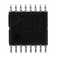
MC908QY1ACDTE Freescale Semiconductor, MC908QY1ACDTE Datasheet - Page 106

MC908QY1ACDTE
Manufacturer Part Number
MC908QY1ACDTE
Description
IC MCU 8BIT 1.5K FLASH 16TSSOP
Manufacturer
Freescale Semiconductor
Series
HC08r
Datasheet
1.MC908QT1ACDWE.pdf
(200 pages)
Specifications of MC908QY1ACDTE
Core Processor
HC08
Core Size
8-Bit
Speed
8MHz
Peripherals
LVD, POR, PWM
Number Of I /o
13
Program Memory Size
1.5KB (1.5K x 8)
Program Memory Type
FLASH
Ram Size
128 x 8
Voltage - Supply (vcc/vdd)
2.7 V ~ 5.5 V
Oscillator Type
Internal
Operating Temperature
-40°C ~ 85°C
Package / Case
16-TSSOP
Processor Series
HC08QY
Core
HC08
Data Bus Width
8 bit
Data Ram Size
128 B
Maximum Clock Frequency
8 MHz
Number Of Programmable I/os
13
Number Of Timers
2
Maximum Operating Temperature
+ 85 C
Mounting Style
SMD/SMT
Development Tools By Supplier
FSICEBASE, M68CBL05AE, DEMO908QB8, DEMO908QC16
Minimum Operating Temperature
- 40 C
Lead Free Status / RoHS Status
Lead free / RoHS Compliant
Eeprom Size
-
Data Converters
-
Connectivity
-
Lead Free Status / Rohs Status
Details
- Current page: 106 of 200
- Download datasheet (2Mb)
Input/Output Ports (PORTS)
12.3.4 Port A Summary Table
The following table summarizes the operation of the port A pins when used as a general-purpose
input/output pins.
12.4 Port B
Port B is an 8-bit special function port that shares two of its pins with the 10-bit ADC (see
Analog-to-Digital Converter (ADC10)
Each port B pin also has a software configurable pullup device if the corresponding port pin is configured
as an input port.
12.4.1 Port B Data Register
The port B data register (PTB) contains a data latch for each of the port B pins.
PTB[7:0] — Port B Data Bits
106
1. X = don’t care
2. I/O pin pulled to V
3. Writing affects data register, but does not affect input.
4. Hi-Z = high impedance
5. Output does not apply to PTA2
PTAPUE
These read/write bits are software programmable. Data direction of each port B pin is under the control
of the corresponding bit in data direction register B. Reset has no effect on port B data.
Bit
X
1
0
Reset:
Read:
Write:
DDRA
Bit
0
0
1
DD
by internal pullup.
PTB7
Bit 7
PTA
X
Bit
X
X
(1)
PTB6
Figure 12-5. Port B Data Register (PTB)
MC68HC908QYA/QTA Family Data Sheet, Rev. 3
6
Input, V
Input, Hi-Z
Table 12-1. Port A Pin Functions
I/O Pin
Output
Mode
Module).
DD
PTB5
5
(2)
(4)
Unaffected by reset
PTB4
4
Accesses to DDRA
DDRA5–DDRA0
DDRA5–DDRA0
DDRA5–DDRA0
Read/Write
PTB3
3
PTB2
2
PTA5–PTA0
PTB1
Read
1
Pin
Pin
Accesses to PTA
Freescale Semiconductor
PTB0
Bit 0
PTA5–PTA0
PTA5–PTA0
PTA5–PTA0
Chapter 3
Write
(3)
(3)
(5)
Related parts for MC908QY1ACDTE
Image
Part Number
Description
Manufacturer
Datasheet
Request
R
Part Number:
Description:
Manufacturer:
Freescale Semiconductor, Inc
Datasheet:
Part Number:
Description:
Manufacturer:
Freescale Semiconductor, Inc
Datasheet:
Part Number:
Description:
Manufacturer:
Freescale Semiconductor, Inc
Datasheet:
Part Number:
Description:
Manufacturer:
Freescale Semiconductor, Inc
Datasheet:
Part Number:
Description:
Manufacturer:
Freescale Semiconductor, Inc
Datasheet:
Part Number:
Description:
Manufacturer:
Freescale Semiconductor, Inc
Datasheet:
Part Number:
Description:
Manufacturer:
Freescale Semiconductor, Inc
Datasheet:
Part Number:
Description:
Manufacturer:
Freescale Semiconductor, Inc
Datasheet:
Part Number:
Description:
Manufacturer:
Freescale Semiconductor, Inc
Datasheet:
Part Number:
Description:
Manufacturer:
Freescale Semiconductor, Inc
Datasheet:
Part Number:
Description:
Manufacturer:
Freescale Semiconductor, Inc
Datasheet:
Part Number:
Description:
Manufacturer:
Freescale Semiconductor, Inc
Datasheet:
Part Number:
Description:
Manufacturer:
Freescale Semiconductor, Inc
Datasheet:
Part Number:
Description:
Manufacturer:
Freescale Semiconductor, Inc
Datasheet:
Part Number:
Description:
Manufacturer:
Freescale Semiconductor, Inc
Datasheet:


