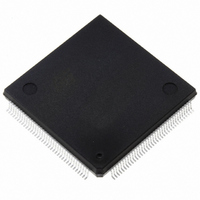
ST10F269Z2Q6 STMicroelectronics, ST10F269Z2Q6 Datasheet - Page 79

ST10F269Z2Q6
Manufacturer Part Number
ST10F269Z2Q6
Description
MCU 16BIT 256K FLASH 144PQFP
Manufacturer
STMicroelectronics
Series
ST10r
Specifications of ST10F269Z2Q6
Core Processor
ST10
Core Size
16-Bit
Speed
40MHz
Connectivity
CAN, EBI/EMI, SSC, UART/USART
Peripherals
POR, PWM, WDT
Number Of I /o
111
Program Memory Size
256KB (256K x 8)
Program Memory Type
FLASH
Ram Size
12K x 8
Voltage - Supply (vcc/vdd)
4.5 V ~ 5.5 V
Data Converters
A/D 16x10b
Oscillator Type
Internal
Operating Temperature
-40°C ~ 85°C
Package / Case
144-QFP
Controller Family/series
ST10
No. Of I/o's
111
Ram Memory Size
12KB
Cpu Speed
40MHz
No. Of Timers
5
Embedded Interface Type
CAN, SSC, USART
Rohs Compliant
Yes
Processor Series
ST10F26x
Core
ST10
Data Bus Width
16 bit
Data Ram Size
12 KB
Interface Type
CAN, SSC, USART
Maximum Clock Frequency
40 MHz
Number Of Programmable I/os
111
Number Of Timers
2 x 16 bit
Operating Supply Voltage
0.3 V to 4 V
Maximum Operating Temperature
+ 85 C
Mounting Style
SMD/SMT
Minimum Operating Temperature
- 40 C
On-chip Adc
16 bit x 10 bit
Lead Free Status / RoHS Status
Lead free / RoHS Compliant
Eeprom Size
-
Lead Free Status / Rohs Status
Details
Other names
497-4833
Available stocks
Company
Part Number
Manufacturer
Quantity
Price
Company:
Part Number:
ST10F269Z2Q6
Manufacturer:
ST
Quantity:
201
Company:
Part Number:
ST10F269Z2Q6
Manufacturer:
ST
Quantity:
745
Company:
Part Number:
ST10F269Z2Q6
Manufacturer:
STMicroelectronics
Quantity:
10 000
Part Number:
ST10F269Z2Q6
Manufacturer:
ST
Quantity:
20 000
Port 5 pins have a special port structure (see Figure 35), first because it is an input only port, and second
because the analog input channels are directly connected to the pins rather than to the input latches.
Figure 35 : Block Diagram of a Port 5 Pin
12.8.2 - Port 5 Schmitt Trigger Analog Inputs
A Schmitt trigger protection can be activated on each pin of Port 5 by setting the dedicated bit of register
P5DIDIS.
P5DIDIS (FFA4h / D2h)
12.9 - Port 6
If this 8-bit port is used for general purpose I/O, the direction of each line can be configured via the
corresponding direction register DP6. Each port line can be switched into push/pull or open drain mode
via the open drain control register ODP6.
DP6 (FFCEH / E7H)
DIS.15
P6 (FFCCh / E6h)
P5DIDIS.y
P6.y
P5DI
RW
15
15
15
-
-
DIS.14
P5DI
RW
14
14
14
-
-
DIS.13
P5DI
RW
13
13
13
-
-
Port 5 Digital Disable Register Bit y
P5DIDIS.y = 0: Port line P5.y digital input is enabled (Schmitt trigger enabled)
P5DIDIS.y = 1: Port line P5.y digital input is disabled (Schmitt trigger disabled,
necessary for input leakage current reduction)
Port Data Register P6 Bit y
DIS.12
P5DI
RW
12
12
12
-
-
DIS.11
P5DI
to Sample + Hold
RW
11
11
11
-
-
Circuit
Read
Buffer
DIS.10
P5DI
RW
10
10
10
-
-
Read Port P5.y
DIS.9
P5DI
RW
9
9
9
-
-
DIS.8
P5DI
RW
Channel
8
8
8
-
-
Select
SFR
SFR
SFR
DP6.7 DP6.6 DP6.5 DP6.4 DP6.3 DP6.2 DP6.1 DP6.0
DIS.7
P5DI
P6.7
RW
RW
RW
Clock
Latch
Input
7
7
7
DIS.6
P5DI
P6.6
RW
RW
RW
6
6
6
Analog
Switch
DIS.5
P5DI
P6.5
RW
RW
RW
5
5
5
DIS.4
P5DI
P6.4
RW
RW
RW
4
4
4
P5.y/ANy
DIS.3
P5DI
P6.3
RW
RW
RW
3
3
3
Reset Value: 0000h
Reset Value: --00h
Reset Value: --00h
DIS.2
P5DI
P6.2
RW
RW
RW
2
2
2
ST10F269-T3
y = 15...0
DIS.1
P5DI
P6.1
RW
RW
RW
1
1
1
79/162
DIS.0
P5DI
P6.0
RW
RW
RW
0
0
0


