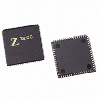
Z86C9620VSG Zilog, Z86C9620VSG Datasheet - Page 24

Z86C9620VSG
Manufacturer Part Number
Z86C9620VSG
Description
IC Z8 20MHZ C91 W/7 PORTS 68PLCC
Manufacturer
Zilog
Series
Z8®r
Datasheet
1.Z86C9620PSC.pdf
(42 pages)
Specifications of Z86C9620VSG
Core Processor
Z8
Core Size
8-Bit
Speed
20MHz
Connectivity
EBI/EMI, UART/USART
Number Of I /o
52
Program Memory Type
ROMless
Ram Size
236 x 8
Voltage - Supply (vcc/vdd)
3 V ~ 5.5 V
Oscillator Type
Internal
Operating Temperature
0°C ~ 70°C
Package / Case
68-PLCC
Processor Series
Z86C9xx
Core
Z8
Data Bus Width
8 bit
Program Memory Size
16 KB
Data Ram Size
236 B
Interface Type
UART
Maximum Clock Frequency
20 MHz
Number Of Programmable I/os
52
Number Of Timers
2
Operating Supply Voltage
3 V to 5.5 V
Maximum Operating Temperature
+ 70 C
Mounting Style
SMD/SMT
Minimum Operating Temperature
0 C
Lead Free Status / RoHS Status
Lead free / RoHS Compliant
Eeprom Size
-
Program Memory Size
-
Data Converters
-
Peripherals
-
Lead Free Status / Rohs Status
Details
Available stocks
Company
Part Number
Manufacturer
Quantity
Price
PIN FUNCTIONS (Continued)
Z86C61/62/96
CMOS Z8 Microcontroller
Port 3 can be configured under software control to provide
the following control functions: handshake for Ports 0 and
2 (/DAV and RDY); four external interrupt request signals
Notes:
HS = Handshake Signals
D = Data Available
R = Ready
Uart Operation
Port 3 lines P30 and P37, can be programmed as serial I/O
lines for full-duplex serial asynchronous receiver/transmit-
ter operation. The bit rate is controlled by the
Counter/Timer0.
The Z86C61/62/96 automatically adds a start bit and two
stop bits to transmitted data (Figure 17). Odd parity is also
available as an option. Eight data bits are always transmit-
ted, regardless of parity selection. If parity is enabled, the
eighth bit is the odd parity bit. An interrupt request (IRQ4)
is generated on all transmitted characters.
24
P30
P31
P32
P33
P34
P35
P36
P37
Pin
T0
T1
OUT
OUT
OUT
OUT
I/O
IN
IN
IN
IN
CTC1
T
T
OUT
IN
Table 6. Port 3 Pin Assignments
IRQ3
IRQ2
IRQ0
IRQ1
IRQ4
IRQ5
Int.
PS003501-0301
P R E L I M I N A R Y
P0 HS
D/R
R/D
(IRQ3-IRQ0); timer input and output signals (T
T
Received data must have a start bit, eight data bits and at
least one stop bit. If parity is on, bit 7 of the received data
is replaced by a parity error flag. Received characters gen-
erate the IRQ3 interrupt request.
Note: UART function is only available in standard timing
mode (i.e., P01M D5 = 0).
OUT
P1 HS
), and Data Memory Select (/DM).
D/R
R/D
P2 HS
D/R
R/D
Serial Out
Serial In
UART
DS97Z8X1600
Ext
DM
IN
Zilog
and


