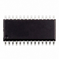
ST72C254G2M6 STMicroelectronics, ST72C254G2M6 Datasheet - Page 76

ST72C254G2M6
Manufacturer Part Number
ST72C254G2M6
Description
IC MCU 8BIT 8K FLASH SOIC-28
Manufacturer
STMicroelectronics
Series
ST7r
Datasheets
1.INDART-ST72C254.pdf
(3 pages)
2.ST72C104G1M6.pdf
(141 pages)
3.ST72C215G2M6.pdf
(140 pages)
Specifications of ST72C254G2M6
Core Processor
ST7
Core Size
8-Bit
Speed
16MHz
Connectivity
I²C, SPI
Peripherals
LVD, POR, PWM, WDT
Number Of I /o
22
Program Memory Size
8KB (8K x 8)
Program Memory Type
FLASH
Ram Size
256 x 8
Voltage - Supply (vcc/vdd)
3.2 V ~ 5.5 V
Data Converters
A/D 6x8b
Oscillator Type
Internal
Operating Temperature
-40°C ~ 85°C
Package / Case
28-SOIC (7.5mm Width)
Controller Family/series
ST7
No. Of I/o's
22
Ram Memory Size
256Byte
Cpu Speed
8MHz
No. Of Timers
2
Rohs Compliant
Yes
Processor Series
ST72C2x
Core
ST7
Data Bus Width
8 bit
Data Ram Size
256 B
Interface Type
I2C, SPI
Maximum Clock Frequency
16 MHz
Number Of Programmable I/os
22
Number Of Timers
3 bit
Operating Supply Voltage
3.2 V to 5.5 V
Maximum Operating Temperature
+ 85 C
Mounting Style
SMD/SMT
Development Tools By Supplier
ST7MDT1-DVP2/US
Minimum Operating Temperature
- 40 C
On-chip Adc
8 bit
Lead Free Status / RoHS Status
Lead free / RoHS Compliant
Eeprom Size
-
Lead Free Status / Rohs Status
In Transition
Available stocks
Company
Part Number
Manufacturer
Quantity
Price
Part Number:
ST72C254G2M6
Manufacturer:
ST
Quantity:
20 000
ST72104Gx, ST72215Gx, ST72216Gx, ST72254Gx
Note: In both cases, SCL line is not held low; how-
ever, the SDA line can remain low if the last bits
transmitted are all 0. It is then necessary to re-
lease both lines by software. The SCL line is not
held low while AF=1 but by other flags (SB or BTF)
that are set at the same time.
How to release the SDA / SCL lines
Set and subsequently clear the STOP bit while
BTF is set. The SDA/SCL lines are released after
the transfer of the current byte.
SMBus Compatibility
ST7 I
supports all SMBus adressing modes, SMBus bus
protocols and CRC-8 packet error checking. Refer
to AN1713: SMBus Slave Driver For ST7 I
ripheral.
11.4.4.2 Master Mode
To switch from default Slave mode to Master
mode a Start condition generation is needed.
Start condition
Setting the START bit while the BUSY bit is
cleared causes the interface to switch to Master
mode (M/SL bit set) and generates a Start condi-
tion.
Once the Start condition is sent:
– The EVF and SB bits are set by hardware with
Then the master waits for a read of the SR1 regis-
ter followed by a write in the DR register with the
Slave address, holding the SCL line low (see
Figure 3
Slave address transmission
Then the slave address is sent to the SDA line via
the internal shift register.
In 7-bit addressing mode, one address byte is
sent.
In 10-bit addressing mode, sending the first byte
including the header sequence causes the follow-
ing event:
– The EVF bit is set by hardware with interrupt
76/141
to correctly handle a second interrupt during the
9th pulse of a transmitted byte.
an interrupt if the ITE bit is set.
generation if the ITE bit is set.
2
C is compatible with SMBus V1.1 protocol. It
Transfer sequencing EV5).
2
C Pe-
Then the master waits for a read of the SR1 regis-
ter followed by a write in the DR register, holding
the SCL line low (see
ing EV9).
Then the second address byte is sent by the inter-
face.
After completion of this transfer (and acknowledge
from the slave if the ACK bit is set):
– The EVF bit is set by hardware with interrupt
Then the master waits for a read of the SR1 regis-
ter followed by a write in the CR register (for exam-
ple set PE bit), holding the SCL line low (see
ure 3
Next the master must enter Receiver or Transmit-
ter mode.
Note: In 10-bit addressing mode, to switch the
master to Receiver mode, software must generate
a repeated Start condition and resend the header
sequence with the least significant bit set
(11110xx1).
Master Receiver
Following the address transmission and after SR1
and CR registers have been accessed, the master
receives bytes from the SDA line into the DR reg-
ister via the internal shift register. After each byte
the interface generates in sequence:
– Acknowledge pulse if the ACK bit is set
– EVF and BTF bits are set by hardware with an in-
Then the interface waits for a read of the SR1 reg-
ister followed by a read of the DR register, holding
the SCL line low (see
ing EV7).
To close the communication: before reading the
last byte from the DR register, set the STOP bit to
generate the Stop condition. The interface goes
automatically back to slave mode (M/SL bit
cleared).
Note: In order to generate the non-acknowledge
pulse after the last received data byte, the ACK bit
must be cleared just before reading the second
last data byte.
generation if the ITE bit is set.
terrupt if the ITE bit is set.
Transfer sequencing EV6).
Figure 3
Figure 3
Transfer sequenc-
Transfer sequenc-
Fig-


