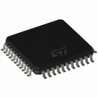
ST72F324J6T6 STMicroelectronics, ST72F324J6T6 Datasheet - Page 80

ST72F324J6T6
Manufacturer Part Number
ST72F324J6T6
Description
IC MCU 8BIT 32K 44-TQFP
Manufacturer
STMicroelectronics
Series
ST7r
Specifications of ST72F324J6T6
Core Processor
ST7
Core Size
8-Bit
Speed
8MHz
Connectivity
SCI, SPI
Peripherals
LVD, POR, PWM, WDT
Number Of I /o
32
Program Memory Size
32KB (32K x 8)
Program Memory Type
FLASH
Ram Size
1K x 8
Voltage - Supply (vcc/vdd)
3.8 V ~ 5.5 V
Data Converters
A/D 12x10b
Oscillator Type
Internal
Operating Temperature
-40°C ~ 85°C
Package / Case
44-TQFP, 44-VQFP
Controller Family/series
ST7
No. Of I/o's
32
Ram Memory Size
1KB
Cpu Speed
8MHz
No. Of Timers
2
Embedded Interface Type
SCI, SPI
No. Of Pwm Channels
1
Rohs Compliant
Yes
Processor Series
ST72F3x
Core
ST7
Data Bus Width
8 bit
Data Ram Size
1024 B
Interface Type
SCI, SPI
Maximum Clock Frequency
8 MHz
Number Of Programmable I/os
32
Number Of Timers
4 bit
Operating Supply Voltage
3.8 V to 5.5 V
Maximum Operating Temperature
+ 85 C
Mounting Style
SMD/SMT
Development Tools By Supplier
ST7F521-IND/USB, ST7232X-EVAL, ST7MDT20-DVP3, ST7MDT20J-EMU3, STX-RLINK
Minimum Operating Temperature
- 40 C
On-chip Adc
10 bit
Cpu Family
ST7
Device Core Size
8b
Frequency (max)
8MHz
Total Internal Ram Size
1KB
# I/os (max)
32
Number Of Timers - General Purpose
2
Operating Supply Voltage (typ)
5V
Operating Supply Voltage (max)
5.5V
Operating Supply Voltage (min)
3.8V
Instruction Set Architecture
CISC
Operating Temp Range
-40C to 85C
Operating Temperature Classification
Industrial
Mounting
Surface Mount
Pin Count
44
Package Type
TQFP
For Use With
497-8222 - UPS (LINE INTERACTIVE - 450W)497-8436 - BOARD EVAL UPS 450W VOUT=220V497-6421 - BOARD EVAL DGTL BATT CHGR DESIGN
Lead Free Status / RoHS Status
Contains lead / RoHS non-compliant
Eeprom Size
-
Lead Free Status / Rohs Status
In Transition
Other names
497-2108
Available stocks
Company
Part Number
Manufacturer
Quantity
Price
Company:
Part Number:
ST72F324J6T6
Manufacturer:
STMicroelectronics
Quantity:
10 000
Part Number:
ST72F324J6T6
Manufacturer:
ST
Quantity:
20 000
Company:
Part Number:
ST72F324J6T6/TR
Manufacturer:
STMicroelectronics
Quantity:
10 000
ST72324Jx ST72324Kx
SERIAL PERIPHERAL INTERFACE (Cont’d)
10.4.3.1 Functional Description
A basic example of interconnections between a
single master and a single slave is illustrated in
Figure
The MOSI pins are connected together and the
MISO pins are connected together. In this way
data is transferred serially between master and
slave (most significant bit first).
Figure 47. Single Master/ Single Slave Application
80/164
1
– SS: Slave select:
This input signal acts as a ‘chip select’ to let
the SPI master communicate with slaves indi-
vidually and to avoid contention on the data
lines. Slave SS inputs can be driven by stand-
ard I/O ports on the master MCU.
47.
MSBit
8-BIT SHIFT REGISTER
GENERATOR
CLOCK
SPI
MASTER
LSBit
SCK
MOSI
SS
MISO
+5V
The communication is always initiated by the mas-
ter. When the master device transmits data to a
slave device via MOSI pin, the slave device re-
sponds by sending data to the master device via
the MISO pin. This implies full duplex communica-
tion with both data out and data in synchronized
with the same clock signal (which is provided by
the master device via the SCK pin).
To use a single data line, the MISO and MOSI pins
must be connected at each node (in this case only
simplex communication is possible).
Four possible data/clock timing relationships may
be chosen (see
must be programmed with the same timing mode.
MISO
MOSI
SCK
SS
Figure
8-BIT SHIFT REGISTER
MSBit
Not used if SS is managed
by software
50) but master and slave
SLAVE
LSBit


