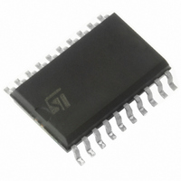
ST72F623F2M1 STMicroelectronics, ST72F623F2M1 Datasheet - Page 50

ST72F623F2M1
Manufacturer Part Number
ST72F623F2M1
Description
IC MCU 8BIT LS 8K 20-SOIC
Manufacturer
STMicroelectronics
Series
ST7r
Datasheet
1.ST72F622L2M1.pdf
(139 pages)
Specifications of ST72F623F2M1
Core Processor
ST7
Core Size
8-Bit
Speed
8MHz
Connectivity
USB
Peripherals
DMA, LVD, POR, PWM, WDT
Number Of I /o
11
Program Memory Size
8KB (8K x 8)
Program Memory Type
FLASH
Ram Size
384 x 8
Voltage - Supply (vcc/vdd)
4 V ~ 5.5 V
Data Converters
A/D 3x10b
Oscillator Type
Internal
Operating Temperature
0°C ~ 70°C
Package / Case
20-SOIC (7.5mm Width)
Processor Series
ST72F6x
Core
ST7
Data Bus Width
8 bit
Data Ram Size
384 B
Interface Type
SCI, SPI, USB
Maximum Clock Frequency
12 MHz
Number Of Programmable I/os
11
Number Of Timers
2
Operating Supply Voltage
4 V to 5.5 V
Maximum Operating Temperature
+ 70 C
Mounting Style
SMD/SMT
Minimum Operating Temperature
0 C
On-chip Adc
10 bit
Lead Free Status / RoHS Status
Contains lead / RoHS non-compliant
Eeprom Size
-
Lead Free Status / Rohs Status
Details
Other names
497-2114-5
Available stocks
Company
Part Number
Manufacturer
Quantity
Price
Company:
Part Number:
ST72F623F2M1
Manufacturer:
NXP
Quantity:
670
Part Number:
ST72F623F2M1
Manufacturer:
ST
Quantity:
20 000
ST7262xxx
PWM AUTO-RELOAD TIMER (Cont’d)
PWM CONTROL REGISTER (PWMCR)
Read/Write
Reset Value: 0000 0000 (00h)
Bit 7:6 = Reserved.
Bit 5:4 = OE[1:0] PWM Output Enable
These bits are set and cleared by software. They
enable or disable the PWM output channels inde-
pendently acting on the corresponding I/O pin.
0: PWM output disabled.
1: PWM output enabled.
Bit 3:2 = Reserved.
Bit 1:0 = OP[1:0] PWM Output Polarity
These bits are set and cleared by software. They
independently select the polarity of the two PWM
output signals.
Notes:
– When an OPx bit is modified, the PWMx output
– If DCRx=FFh then the output level is always 0.
– If DCRx=00h then the output level is always 1.
50/139
signal polarity is immediately reversed.
Counter <= OCRx
7
0
0
1
0
PWMx output level
OE1
OE0
Counter > OCRx
0
0
1
0
OP1
OPx
OP0
0
1
0
Doc ID 6996 Rev 5
DUTY CYCLE REGISTERS (DCRx)
Read/Write
Reset Value: 0000 0000 (00h)
Bit 7:0 = DC[7:0] Duty Cycle Data
These bits are set and cleared by software.
A DCRx register is associated with the OCRx reg-
ister of each PWM channel to determine the sec-
ond edge location of the PWM signal (the first
edge location is common to all channels and given
by the ARR register). These DCR registers allow
the duty cycle to be set independently for each
PWM channel.
DC7
7
DC6
DC5
DC4
DC3
DC2
DC1
DC0
0


