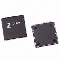
Z8F2422VS020SG Zilog, Z8F2422VS020SG Datasheet - Page 178

Z8F2422VS020SG
Manufacturer Part Number
Z8F2422VS020SG
Description
IC ENCORE MCU FLASH 24K 68PLCC
Manufacturer
Zilog
Series
Encore!® XP®r
Specifications of Z8F2422VS020SG
Core Processor
Z8
Core Size
8-Bit
Speed
20MHz
Connectivity
I²C, IrDA, SPI, UART/USART
Peripherals
Brown-out Detect/Reset, DMA, POR, PWM, WDT
Number Of I /o
46
Program Memory Size
24KB (24K x 8)
Program Memory Type
FLASH
Ram Size
2K x 8
Voltage - Supply (vcc/vdd)
3 V ~ 3.6 V
Data Converters
A/D 12x10b
Oscillator Type
Internal
Operating Temperature
0°C ~ 70°C
Package / Case
68-LCC (J-Lead)
Processor Series
Z8F242x
Core
eZ8
Data Bus Width
8 bit
Data Ram Size
2 KB
Interface Type
I2C, SPI, UART
Maximum Clock Frequency
20 MHz
Number Of Programmable I/os
46
Number Of Timers
4
Operating Supply Voltage
3 V to 3.6 V
Maximum Operating Temperature
+ 70 C
Mounting Style
SMD/SMT
Development Tools By Supplier
Z8F64200100KITG, ZENETSC0100ZACG, ZUSBSC00100ZACG, Z8F64210100ZDA, Z8F64210100ZDP, Z8F64210100ZDV, Z8F64220100ZDA, Z8F64220100ZDV, Z8F6422AR00ZEM, Z8F6422VS00ZEM, Z8F6421AN00ZEM
Minimum Operating Temperature
0 C
On-chip Adc
10 bit, 12 Channel
Lead Free Status / RoHS Status
Lead free / RoHS Compliant
Eeprom Size
-
Lead Free Status / Rohs Status
Details
Other names
269-4253
Z8F2422VS020SG
Z8F2422VS020SG
Available stocks
Company
Part Number
Manufacturer
Quantity
Price
- Current page: 178 of 297
- Download datasheet (9Mb)
PS019921-0308
DMAx I/O Address Register
1 = DMAx, after the End Address data is transferred, reloads the original Start
DDIR—DMAx Data Transfer Direction
0 = Register File → on-chip peripheral control register.
1 = on-chip peripheral control register → Register File.
IRQEN—DMAx Interrupt Enable
0 = DMAx does not generate any interrupts.
1 = DMAx generates an interrupt when the End Address data is transferred.
WSEL—Word Select
0 = DMAx transfers a single byte per request.
1 = DMAx transfers a two-byte word per request. The address for the on-chip
RSS—Request Trigger Source Select
The Request Trigger Source Select field determines the peripheral that can initiate a DMA
transfer. The corresponding interrupts do not need to be enabled within the Interrupt Con-
troller to initiate a DMA transfer. However, if the Request Trigger Source can enable or
disable the interrupt request sent to the Interrupt Controller, the interrupt request must be
enabled within the Request Trigger Source block.
000 = Timer 0.
001 = Timer 1.
010 = Timer 2.
011 = Timer 3.
100 = DMA0 Control register: UART0 Received Data register contains valid data.
101 = DMA0 Control register: UART1 Received Data register contains valid data. DMA1
Control register: UART1 Transmit Data register empty.
110 = DMA0 Control register: I
111 = Reserved.
The DMAx I/O Address register
address for data transfer. The full 12-bit Register File address is given by {FH,
Address and continues operating.
peripheral control register must be an even address.
DMA1 Control register: UART0 Transmit Data register empty.
Transmitter Interrupt register empty.
2
(Table
C Receiver Interrupt. DMA1 Control register: I
78) contains the low byte of the on-chip peripheral
Z8 Encore! XP
Direct Memory Access Controller
Product Specification
®
F64XX Series
2
C
164
Related parts for Z8F2422VS020SG
Image
Part Number
Description
Manufacturer
Datasheet
Request
R

Part Number:
Description:
Communication Controllers, ZILOG INTELLIGENT PERIPHERAL CONTROLLER (ZIP)
Manufacturer:
Zilog, Inc.
Datasheet:

Part Number:
Description:
KIT DEV FOR Z8 ENCORE 16K TO 64K
Manufacturer:
Zilog
Datasheet:

Part Number:
Description:
KIT DEV Z8 ENCORE XP 28-PIN
Manufacturer:
Zilog
Datasheet:

Part Number:
Description:
DEV KIT FOR Z8 ENCORE 8K/4K
Manufacturer:
Zilog
Datasheet:

Part Number:
Description:
KIT DEV Z8 ENCORE XP 28-PIN
Manufacturer:
Zilog
Datasheet:

Part Number:
Description:
DEV KIT FOR Z8 ENCORE 4K TO 8K
Manufacturer:
Zilog
Datasheet:

Part Number:
Description:
CMOS Z8 microcontroller. ROM 16 Kbytes, RAM 256 bytes, speed 16 MHz, 32 lines I/O, 3.0V to 5.5V
Manufacturer:
Zilog, Inc.
Datasheet:

Part Number:
Description:
Low-cost microcontroller. 512 bytes ROM, 61 bytes RAM, 8 MHz
Manufacturer:
Zilog, Inc.
Datasheet:

Part Number:
Description:
Z8 4K OTP Microcontroller
Manufacturer:
Zilog, Inc.
Datasheet:

Part Number:
Description:
CMOS SUPER8 ROMLESS MCU
Manufacturer:
Zilog, Inc.
Datasheet:

Part Number:
Description:
SL1866 CMOSZ8 OTP Microcontroller
Manufacturer:
Zilog, Inc.
Datasheet:

Part Number:
Description:
SL1866 CMOSZ8 OTP Microcontroller
Manufacturer:
Zilog, Inc.
Datasheet:

Part Number:
Description:
OTP (KB) = 1, RAM = 125, Speed = 12, I/O = 14, 8-bit Timers = 2, Comm Interfaces Other Features = Por, LV Protect, Voltage = 4.5-5.5V
Manufacturer:
Zilog, Inc.
Datasheet:

Part Number:
Description:
Manufacturer:
Zilog, Inc.
Datasheet:


