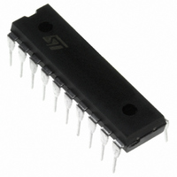
ST7FLITE25F1B6 STMicroelectronics, ST7FLITE25F1B6 Datasheet - Page 107

ST7FLITE25F1B6
Manufacturer Part Number
ST7FLITE25F1B6
Description
IC MCU 8BIT 8K FLASH 20-DIP
Manufacturer
STMicroelectronics
Series
ST7r
Specifications of ST7FLITE25F1B6
Core Processor
ST7
Core Size
8-Bit
Speed
8MHz
Connectivity
SPI
Peripherals
LVD, POR, PWM, WDT
Number Of I /o
15
Program Memory Size
8KB (8K x 8)
Program Memory Type
FLASH
Ram Size
384 x 8
Voltage - Supply (vcc/vdd)
2.4 V ~ 5.5 V
Data Converters
A/D 7x10b
Oscillator Type
Internal
Operating Temperature
-40°C ~ 85°C
Package / Case
20-DIP (0.300", 7.62mm)
Processor Series
ST7FLITE2x
Core
ST7
Data Bus Width
8 bit
Development Tools By Supplier
ST7FLITE-SK/RAIS, ST7MDT10-DVP3, ST7MDT10-EMU3, STX-RLINK
For Use With
497-5858 - EVAL BOARD PLAYBACK ST7FLITE
Lead Free Status / RoHS Status
Lead free / RoHS Compliant
Eeprom Size
-
Lead Free Status / Rohs Status
Details
Available stocks
Company
Part Number
Manufacturer
Quantity
Price
I/O PORT PIN CHARACTERISTICS (Cont’d)
13.8.2 Output Driving Current
Subject to general operating conditions for V
Notes:
1. The I
(I/O ports and control pins) must not exceed I
2. The I
I
3. Not tested in production, based on characterization results.
Figure 69. Typical V
IO
Symbol
V
V
V
V
V
V
OH
OH
(I/O ports and control pins) must not exceed I
OL
OL
OH
0.70
0.60
0.50
0.40
0.30
0.20
0.10
0.00
OL
1)3)
1)3)
2)3)
2)3)
1)
2)
IO
IO
current sourced must always respect the absolute maximum rating specified in
current sunk must always respect the absolute maximum rating specified in
Output low level voltage for a standard I/O pin
when 8 pins are sunk at same time
(see
Output low level voltage for a high sink I/O pin
when 4 pins are sunk at same time
Output high level voltage for an I/O pin
when 4 pins are sourced at same time
Output low level voltage for a standard I/O pin
when 8 pins are sunk at same time
(see
Output low level voltage for a high sink I/O pin
when 4 pins are sunk at same time
Output high level voltage for an I/O pin
when 4 pins are sourced at same time
(see
Output low level voltage for a standard I/O pin
when 8 pins are sunk at same time
(see
Output low level voltage for a high sink I/O pin
when 4 pins are sunk at same time
(see
Output high level voltage for an I/O pin
when 4 pins are sourced at same time
(see
0.01
TO BE CHARACTERIZED
Figure
Figure
Figure
Figure
Figure
Figure
71)
70)
77)
OL
72)
74)
80)
lio (mA)
1
at V
Parameter
DD
=2.4V (standard)
2
VSS
VDD
.
DD
.
-45
0°C
25°C
90°C
130°C
, f
CPU
, and T
Figure 70. Typical V
0.60
0.50
0.40
0.30
0.20
0.10
0.00
I
I
I
I
I
I
I
I
I
I
I
I
IO
IO
IO
IO
IO
IO
IO
IO
IO
IO
IO
IO
A
Conditions
=+5mA T
=+2mA T
=+20mA, T
=+8mA T
=-5mA, T
=-2mA
=+2mA T
=+8mA T
=-2mA
=+2mA T
=+8mA T
=-2mA
unless otherwise specified.
0.01
T
T
T
T
T
T
T
T
T
T
T
T
T
T
T
A
A
A
A
A
A
A
A
A
A
A
A
A
A
A
A
A
A
A
A
A
A
A
A
≤85°C
≥85°C
≤85°C
≥85°C
≤85°C
≥85°C
≤85°C
≥85°C
≤85°C
≥85°C
≤85°C
≥85°C
≤85°C
≥85°C
≤85°C
≥85°C
≤85°C
≥85°C
≤85°C
≥85°C
≤85°C
≥85°C
≤85°C
≥85°C
Section 13.2.2
OL
lio (mA)
1
Section 13.2.2
V
V
V
V
V
V
V
V
at V
DD
DD
DD
DD
DD
DD
DD
DD
Min
-1.5
-1.6
-0.8
-1.0
-0.8
-1.0
-0.9
-1.0
DD
=2.7V (standard)
and the sum of I
Max
0.75
0.85
2
1.0
1.2
0.4
0.5
1.3
1.5
0.5
0.6
0.5
0.6
0.6
0.7
0.6
0.7
and the sum of
ST7LITE2
107/133
Unit
V
-45°C
0°C
25°C
90°C
130°C
IO


