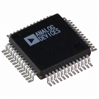
ADUC812BSZ Analog Devices Inc, ADUC812BSZ Datasheet - Page 23

ADUC812BSZ
Manufacturer Part Number
ADUC812BSZ
Description
IC ADC 12BIT MULTICH MCU 52-MQFP
Manufacturer
Analog Devices Inc
Series
MicroConverter® ADuC8xxr
Datasheet
1.EVAL-ADUC812QS.pdf
(60 pages)
Specifications of ADUC812BSZ
Core Size
8-Bit
Program Memory Size
8KB (8K x 8)
Core Processor
8052
Speed
16MHz
Connectivity
I²C, SPI, UART/USART
Peripherals
PSM, Temp Sensor, WDT
Number Of I /o
34
Program Memory Type
FLASH
Eeprom Size
640 x 8
Ram Size
256 x 8
Voltage - Supply (vcc/vdd)
2.7 V ~ 5.5 V
Data Converters
A/D 8x12b, D/A 2x12b
Oscillator Type
Internal
Operating Temperature
-40°C ~ 85°C
Package / Case
52-MQFP, 52-PQFP
Controller Family/series
(8051) 8052
No. Of I/o's
32
Eeprom Memory Size
8KB
Ram Memory Size
256Byte
Cpu Speed
1.3MIPS
No. Of Timers
3
Package
52MQFP
Device Core
8052
Family Name
ADuC8xx
Maximum Speed
16 MHz
Operating Supply Voltage
3.3|5 V
Data Bus Width
8 Bit
Number Of Programmable I/os
32
Interface Type
I2C/SPI/TWI/UART
On-chip Adc
8-chx12-bit
On-chip Dac
2-chx12-bit
Number Of Timers
3
Lead Free Status / RoHS Status
Lead free / RoHS Compliant
Available stocks
Company
Part Number
Manufacturer
Quantity
Price
Company:
Part Number:
ADUC812BSZ
Manufacturer:
ADI
Quantity:
2 400
Company:
Part Number:
ADUC812BSZ
Manufacturer:
Analog Devices Inc
Quantity:
10 000
Part Number:
ADUC812BSZ
Manufacturer:
ADI/亚德诺
Quantity:
20 000
Company:
Part Number:
ADUC812BSZ-REEL
Manufacturer:
Analog Devices Inc
Quantity:
10 000
To drive significant loads with the DAC outputs, external
buffering may be required, as illustrated in Figure 22.
The DAC output buffer also features a high impedance disable
function. In the chip’s default power-on state, both DACs are
disabled, and their outputs are in a high impedance state (or
“three-state”) where they remain inactive until enabled in software.
This means that if a zero output is desired during power-up or
power-down transient conditions, then a pull-down resistor must
be added to each DAC output. Assuming this resistor is in place,
REV. E
Figure 21. Source and Sink Current Capability with
V
REF
= V
3
2
1
0
0
Figure 22. Buffering the DAC Outputs
DD
= 3 V
SOURCE/SINK CURRENT – mA
5
10
9
10
ADuC812
15
–23–
the DAC outputs will remain at ground potential whenever the
DAC is disabled. However, each DAC output will still spike
briefly when power is first applied to the chip, and again when
each DAC is first enabled in software. Typical scope shots of
these spikes are given in Figure 23 and Figure 24, respectively.
Figure 23. DAC Output Spike at Chip Power-Up
Figure 24. DAC Output Spike at DAC Enable
5
200 s/DIV
s/DIV, 1V/DIV
DAC OUT – 500mV/DIV
AV
DD
ADuC812
– 2V/DIV


