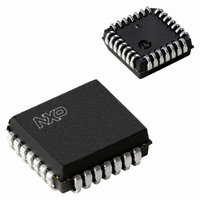
P89LPC932A1FA,112 NXP Semiconductors, P89LPC932A1FA,112 Datasheet - Page 33

P89LPC932A1FA,112
Manufacturer Part Number
P89LPC932A1FA,112
Description
IC 80C51 MCU FLASH 8K 28-PLCC
Manufacturer
NXP Semiconductors
Series
LPC900r
Datasheet
1.P89LPC932A1FDH529.pdf
(64 pages)
Specifications of P89LPC932A1FA,112
Core Processor
8051
Core Size
8-Bit
Speed
18MHz
Connectivity
I²C, SPI, UART/USART
Peripherals
Brown-out Detect/Reset, LED, POR, PWM, WDT
Number Of I /o
26
Program Memory Size
8KB (8K x 8)
Program Memory Type
FLASH
Ram Size
768 x 8
Voltage - Supply (vcc/vdd)
2.4 V ~ 3.6 V
Oscillator Type
Internal
Operating Temperature
-40°C ~ 85°C
Package / Case
28-PLCC
Processor Series
P89LPC9x
Core
80C51
Data Bus Width
8 bit
Data Ram Size
768 B
Interface Type
I2C, SPI, UART
Maximum Clock Frequency
12 MHz
Number Of Programmable I/os
26
Number Of Timers
2
Operating Supply Voltage
2.4 V to 3.6 V
Maximum Operating Temperature
+ 85 C
Mounting Style
SMD/SMT
3rd Party Development Tools
PK51, CA51, A51, ULINK2
Minimum Operating Temperature
- 40 C
For Use With
OM6292 - DEMO BOARD PCA2125 RTCDB-TSSOP-LPC932 - BOARD FOR LPC932 TSSOP622-1014 - BOARD FOR LPC9XX TSSOP622-1008 - BOARD FOR LPC9103 10-HVSON622-1006 - SOCKET ADAPTER BOARDMCB900K - BOARD PROTOTYPE NXP 89LPC9EPM900K - EMULATOR/PROGRAMMER NXP P89LPC9568-4000 - DEMO BOARD SPI/I2C TO DUAL UART568-3510 - DEMO BOARD SPI/I2C TO UART622-1003 - KIT FOR LCD DEMO622-1002 - USB IN-CIRCUIT PROG LPC9XX568-1759 - EMULATOR DEBUGGER/PROGRMMR LPC9X568-1758 - BOARD EVAL FOR LPC93X MCU FAMILY
Lead Free Status / RoHS Status
Lead free / RoHS Compliant
Eeprom Size
-
Data Converters
-
Lead Free Status / Rohs Status
Details
Other names
568-4279-5
935276131112
P89LPC932A1FA
935276131112
P89LPC932A1FA
Available stocks
Company
Part Number
Manufacturer
Quantity
Price
Company:
Part Number:
P89LPC932A1FA,112
Manufacturer:
NXP Semiconductors
Quantity:
10 000
NXP Semiconductors
P89LPC932A1_3
Product data sheet
7.21 I
The I
connected to the bus, and it has the following features:
A typical I
a byte-oriented I
2
Fig 14. I
•
•
•
•
•
•
C-bus serial interface
Bidirectional data transfer between masters and slaves.
Multi master bus (no central master).
Arbitration between simultaneously transmitting masters without corruption of serial
data on the bus.
Serial clock synchronization allows devices with different bit rates to communicate via
one serial bus.
Serial clock synchronization can be used as a handshake mechanism to suspend and
resume serial transfer.
The I
2
C-bus uses two wires (SDA and SCL) to transfer information between devices
2
2
2
C-bus configuration
C-bus may be used for test and diagnostic purposes.
C-bus configuration is shown in
I
2
C-bus
2
C-bus interface that supports data transfers up to 400 kHz.
P1.3/SDA
Rev. 03 — 12 March 2007
P89LPC932A1
8-bit microcontroller with accelerated two-clock 80C51 core
P1.2/SCL
OTHER DEVICE
WITH I
R
Figure
INTERFACE
P
2
C-BUS
14. The P89LPC932A1 device provides
R
P
OTHER DEVICE
P89LPC932A1
WITH I
INTERFACE
2
C-BUS
002aaa898
© NXP B.V. 2007. All rights reserved.
SDA
SCL
33 of 64


