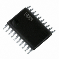
P89LPC9221FDH,512 NXP Semiconductors, P89LPC9221FDH,512 Datasheet - Page 8

P89LPC9221FDH,512
Manufacturer Part Number
P89LPC9221FDH,512
Description
IC 80C51 MCU FLASH 8K 20-TSSOP
Manufacturer
NXP Semiconductors
Series
LPC900r
Datasheet
1.P89LPC921FN112.pdf
(46 pages)
Specifications of P89LPC9221FDH,512
Program Memory Type
FLASH
Program Memory Size
8KB (8K x 8)
Package / Case
20-TSSOP
Core Processor
8051
Core Size
8-Bit
Speed
18MHz
Connectivity
I²C, UART/USART
Peripherals
Brown-out Detect/Reset, LED, POR, PWM, WDT
Number Of I /o
18
Ram Size
256 x 8
Voltage - Supply (vcc/vdd)
2.4 V ~ 3.6 V
Oscillator Type
Internal
Operating Temperature
-40°C ~ 85°C
Processor Series
P89LPC
Core
80C51
Data Bus Width
8 bit
Data Ram Size
256 B
Interface Type
I2C, SPI, UART
Maximum Clock Frequency
18 MHz
Number Of Programmable I/os
15
Operating Supply Voltage
2.4 V to 3.6 V
Maximum Operating Temperature
+ 85 C
Mounting Style
SMD/SMT
3rd Party Development Tools
PK51, CA51, A51, ULINK2
Minimum Operating Temperature
- 40 C
Lead Free Status / RoHS Status
Lead free / RoHS Compliant
For Use With
622-1014 - BOARD FOR LPC9XX TSSOP622-1010 - BOARD FOR LPC922 TSSOP622-1008 - BOARD FOR LPC9103 10-HVSON622-1006 - SOCKET ADAPTER BOARDEPM900K - EMULATOR/PROGRAMMER NXP P89LPC9568-4000 - DEMO BOARD SPI/I2C TO DUAL UART568-3510 - DEMO BOARD SPI/I2C TO UART568-1759 - EMULATOR DEBUGGER/PROGRMMR LPC9X
Eeprom Size
-
Data Converters
-
Lead Free Status / Rohs Status
Lead free / RoHS Compliant
Other names
568-3223-5
935278674512
P89LPC9221FDH
935278674512
P89LPC9221FDH
Philips Semiconductors
Table 3:
[1]
6. Logic symbol
9397 750 14469
Product data
Symbol
P3.0 to P3.1
V
V
Fig 4. Logic symbol.
SS
DD
Input/Output for P1.0-P1.4, P1.6, P1.7. Input for P1.5.
Pin description
Pin
7
6
5
15
CLKOUT
KBI0
KBI1
KBI2
KBI3
KBI4
KBI5
KBI6
KBI7
Type
I/O
I/O
O
O
I/O
I
I
I
…continued
CMPREF
CIN2B
CIN2A
CIN1B
CIN1A
XTAL2
XTAL1
CMP2
CMP1
Description
Port 3: Port 3 is an 2-bit I/O port with a user-configurable output type. During reset
Port 3 latches are configured in the input only mode with the internal pull-up disabled.
The operation of Port 3 pins as inputs and outputs depends upon the port configuration
selected. Each port pin is configured independently. Refer to
configurations”
All pins have Schmitt triggered inputs.
Port 3 also provides various special functions as described below:
P3.0 — Port 3 bit 0.
XTAL2 — Output from the oscillator amplifier (when a crystal oscillator option is
selected via the FLASH configuration.
CLKOUT — CPU clock divided by 2 when enabled via SFR bit (ENCLK - TRIM.6). It
can be used if the CPU clock is the internal RC oscillator, watchdog oscillator or
external clock input, except when XTAL1/XTAL2 are used to generate clock source for
the real time clock/system timer.
P3.1 — Port 3 bit 1.
XTAL1 — Input to the oscillator circuit and internal clock generator circuits (when
selected via the FLASH configuration). It can be a port pin if internal RC oscillator or
watchdog oscillator is used as the CPU clock source, and if XTAL1/XTAL2 are not used
to generate the clock for the real time clock/system timer.
Ground: 0 V reference.
Power Supply: This is the power supply voltage for normal operation as well as Idle
and Power down modes.
T1
Rev. 08 — 15 December 2004
and
Table 8 “DC electrical characteristics”
V DD
P89LPC920/921/922/9221
002aaa409
V SS
8-bit microcontrollers with two-clock 80C51 core
© Koninklijke Philips Electronics N.V. 2004. All rights reserved.
TxD
RxD
T0
INT0
INT1
RST
for details.
Section 8.12.1 “Port
SCL
SDA
8 of 46


