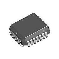
P89LPC982FA,529 NXP Semiconductors, P89LPC982FA,529 Datasheet - Page 10

P89LPC982FA,529
Manufacturer Part Number
P89LPC982FA,529
Description
MCU 80C51 8KB FLASH 28PLCC
Manufacturer
NXP Semiconductors
Series
LPC900r
Datasheet
1.P89LPC980FDH529.pdf
(85 pages)
Specifications of P89LPC982FA,529
Program Memory Type
FLASH
Program Memory Size
8KB (8K x 8)
Package / Case
28-PLCC
Core Processor
8051
Core Size
8-Bit
Speed
18MHz
Connectivity
I²C, SPI, UART/USART
Peripherals
Brown-out Detect/Reset, POR, PWM, WDT
Number Of I /o
26
Ram Size
512 x 8
Voltage - Supply (vcc/vdd)
2.4 V ~ 5.5 V
Oscillator Type
Internal
Operating Temperature
-40°C ~ 85°C
Processor Series
P89LPC
Core
80C51
Data Bus Width
8 bit
Data Ram Size
256 B
Interface Type
I2C, SPI, UART
Maximum Clock Frequency
18 MHz
Number Of Programmable I/os
23
Number Of Timers
5
Operating Supply Voltage
2.4 V to 5.5 V
Maximum Operating Temperature
+ 85 C
Mounting Style
SMD/SMT
3rd Party Development Tools
PK51, CA51, A51, ULINK2
Minimum Operating Temperature
- 40 C
Lead Free Status / RoHS Status
Lead free / RoHS Compliant
Eeprom Size
-
Data Converters
-
Lead Free Status / Rohs Status
Lead free / RoHS Compliant
Other names
935290304529
Available stocks
Company
Part Number
Manufacturer
Quantity
Price
Company:
Part Number:
P89LPC982FA,529
Manufacturer:
NXP Semiconductors
Quantity:
10 000
NXP Semiconductors
Table 3.
P89LPC980_982_983_985
Product data sheet
Symbol
P0.0 to P0.7
P0.0/CMP2/KBI0/
AD05/SPICLK
P0.1/CIN2B/
KBI1/AD00
P0.2/CIN2A/
KBI2/AD01
P0.3/CIN1B/
KBI3/AD02/T2
P0.4/CIN1A/
KBI4/AD03
P0.5/CMPREF/
KBI5/T3
Pin description
6.2 Pin description
Pin
PLCC28,
TSSOP28
3
26
25
24
23
22
Type Description
I/O
I/O
O
I
I
I/O
I/O
I
I
I
I/O
I
I
I
I/O
I
I
I
I/O
I/O
I
I
I
I/O
I
I
I/O
Port 0: Port 0 is an 8-bit I/O port with a user-configurable output type. During reset
Port 0 latches are configured in the input only mode with the internal pull-up
disabled. The operation of Port 0 pins as inputs and outputs depends upon the port
configuration selected. Each port pin is configured independently. Refer to
7.16.1 “Port configurations”
The Keypad Interrupt feature operates with Port 0 pins.
All pins have Schmitt trigger inputs.
Port 0 also provides various special functions as described below:
P0.0 — Port 0 bit 0.
CMP2 — Comparator 2 output
KBI0 — Keyboard input 0.
AD05 — ADC0 channel 5 analog input. (P89LPC985)
SPICLK — SPI clock. When configured as master, this pin is output; when
configured as slave, this pin is input. (pin remap)
P0.1 — Port 0 bit 1.
CIN2B — Comparator 2 positive input B.
KBI1 — Keyboard input 1.
AD00 — ADC0 channel 0 analog input. (P89LPC983/985)
P0.2 — Port 0 bit 2.
CIN2A — Comparator 2 positive input A.
KBI2 — Keyboard input 2.
AD01 — ADC0 channel 1 analog input. (P89LPC983/985)
P0.3 — Port 0 bit 3. High current source.
CIN1B — Comparator 1 positive input B.
KBI3 — Keyboard input 3.
AD02 — ADC0 channel 2 analog input. (P89LPC983/985)
T2 — Timer/counter 2 external count input or overflow output.
P0.4 — Port 0 bit 4. High current source.
CIN1A — Comparator 1 positive input A.
KBI4 — Keyboard input 4.
AD03 — ADC0 channel 3 analog input. (P89LPC983/985)
P0.5 — Port 0 bit 5. High current source.
CMPREF — Comparator reference (negative) input.
KBI5 — Keyboard input 5.
T3 — Timer/counter 3 external count input or overflow output.
Rev. 4 — 15 June 2010
8-bit microcontroller with accelerated two-clock 80C51 core
P89LPC980/982/983/985
and
Table 13 “Static characteristics”
© NXP B.V. 2010. All rights reserved.
for details.
Section
10 of 85


