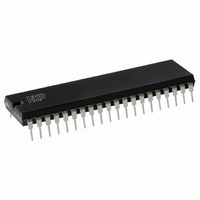
P80C32X2FN,112 NXP Semiconductors, P80C32X2FN,112 Datasheet - Page 44

P80C32X2FN,112
Manufacturer Part Number
P80C32X2FN,112
Description
IC 80C51 MCU 256 ROMLESS 40DIP
Manufacturer
NXP Semiconductors
Series
80Cr
Datasheet
1.P87C52X2BN112.pdf
(62 pages)
Specifications of P80C32X2FN,112
Core Processor
8051
Core Size
8-Bit
Speed
33MHz
Connectivity
EBI/EMI, UART/USART
Peripherals
POR
Number Of I /o
32
Program Memory Type
ROMless
Ram Size
256 x 8
Voltage - Supply (vcc/vdd)
2.7 V ~ 5.5 V
Oscillator Type
Internal
Operating Temperature
-40°C ~ 85°C
Package / Case
40-DIP (0.600", 15.24mm)
Cpu Family
80C
Device Core
80C51
Device Core Size
8b
Frequency (max)
33MHz
Interface Type
UART
Program Memory Size
Not Required
Total Internal Ram Size
256Byte
# I/os (max)
32
Number Of Timers - General Purpose
3
Operating Supply Voltage (typ)
5V
Operating Supply Voltage (max)
5.5V
Operating Supply Voltage (min)
4.5V
Instruction Set Architecture
CISC
Operating Temp Range
-40C to 85C
Operating Temperature Classification
Industrial
Mounting
Through Hole
Pin Count
40
Package Type
PDIP
Processor Series
P80C3x
Core
80C51
Data Bus Width
8 bit
Data Ram Size
256 B
Maximum Clock Frequency
33 MHz
Number Of Programmable I/os
32
Number Of Timers
3
Operating Supply Voltage
2.7 V to 5.5 V
Maximum Operating Temperature
+ 85 C
Mounting Style
Through Hole
3rd Party Development Tools
PK51, CA51, A51, ULINK2
Minimum Operating Temperature
- 40 C
Lead Free Status / RoHS Status
Lead free / RoHS Compliant
Eeprom Size
-
Program Memory Size
-
Data Converters
-
Lead Free Status / Rohs Status
Compliant
Other names
935269611112
P80C32X2FN
P80C32X2FN
P80C32X2FN
P80C32X2FN
Available stocks
Company
Part Number
Manufacturer
Quantity
Price
Company:
Part Number:
P80C32X2FN,112
Manufacturer:
HONGFA
Quantity:
16 000
Philips Semiconductors
EXPLANATION OF THE AC SYMBOLS
Each timing symbol has five characters. The first character is always
‘t’ (= time). The other characters, depending on their positions,
indicate the name of a signal or the logical status of that signal. The
designations are:
A – Address
C – Clock
D – Input data
H – Logic level high
I – Instruction (program memory contents)
L – Logic level low, or ALE
2003 Jan 24
PORT 0
PORT 2
80C51 8-bit microcontroller family
4K/8K/16K/32K ROM/OTP, low voltage (2.7 to 5.5 V),
low power, high speed (30/33 MHz)
PSEN
ALE
RD
PORT 0
PORT 2
PSEN
ALE
t
AVLL
FROM RI OR DPL
A0–A7
t
LLAX
t
t
AVWL
LHLL
t
t
LLWL
AVLL
A0–A7
Figure 27. External Program Memory Read Cycle
t
t
AVDV
P2.0–P2.7 OR A8–A15 FROM DPF
RLAZ
Figure 28. External Data Memory Read Cycle
t
LLDV
t
t
t
AVIV
LLAX
LLPL
t
LLIV
t
t
PLIV
RLDV
A0–A15
t
PLAZ
t
PLPH
t
RLRH
t
PXIX
INSTR IN
44
t
RHDX
DATA IN
P – PSEN
Q – Output data
R – RD signal
t – Time
V – Valid
W – WR signal
X – No longer a valid logic level
Z – Float
Examples: t
t
PXIZ
t
RHDZ
t
t
AVLL
WHLH
LLPL
= Time for address valid to ALE low.
=Time for ALE low to PSEN low.
A0–A7
A0–A7 FROM PCL
A0–A15 FROM PCH
P80C3xX2; P80C5xX2;
A8–A15
P87C5xX2
SU00006
INSTR IN
Product data
SU00025


