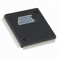
AT91SAM9260B-QU Atmel, AT91SAM9260B-QU Datasheet - Page 14

AT91SAM9260B-QU
Manufacturer Part Number
AT91SAM9260B-QU
Description
IC ARM9 MCU 208-PQFP
Manufacturer
Atmel
Series
AT91SAMr
Specifications of AT91SAM9260B-QU
Core Processor
ARM9
Core Size
16/32-Bit
Speed
180MHz
Connectivity
EBI/EMI, Ethernet, I²C, MMC, SPI, SSC, UART/USART, USB
Peripherals
POR, WDT
Number Of I /o
96
Program Memory Size
32KB (32K x 8)
Program Memory Type
ROM
Ram Size
24K x 8
Voltage - Supply (vcc/vdd)
1.65 V ~ 1.95 V
Data Converters
A/D 4x10b
Oscillator Type
Internal
Operating Temperature
-40°C ~ 85°C
Package / Case
208-MQFP, 208-PQFP
Package
208PQFP
Device Core
ARM926EJ-S
Family Name
91S
Maximum Speed
180 MHz
Operating Supply Voltage
1.8|3.3 V
Data Bus Width
32 Bit
Number Of Programmable I/os
96
Interface Type
EBI/Ethernet/SPI/TWI/UART/USART/USB
On-chip Adc
4-chx10-bit
Number Of Timers
6
Processor Series
AT91SAMx
Core
ARM926EJ-S
Data Ram Size
8 KB
Maximum Clock Frequency
180 MHz
Maximum Operating Temperature
+ 85 C
Mounting Style
SMD/SMT
3rd Party Development Tools
JTRACE-ARM-2M, MDK-ARM, RL-ARM, ULINK2
Development Tools By Supplier
AT91SAM-ICE, AT91-ISP, AT91SAM9260-EK
Minimum Operating Temperature
- 40 C
Cpu Family
AT91
Device Core Size
32b
Frequency (max)
180MHz
Total Internal Ram Size
8KB
# I/os (max)
96
Number Of Timers - General Purpose
6
Operating Supply Voltage (typ)
1.8/3.3V
Operating Supply Voltage (max)
1.95/3.6V
Operating Supply Voltage (min)
1.65/3V
Instruction Set Architecture
RISC
Operating Temp Range
-40C to 85C
Operating Temperature Classification
Industrial
Mounting
Surface Mount
Pin Count
208
Package Type
PQFP
For Use With
AT91SAM9260-EK - KIT EVAL FOR AT91SAM9260AT91SAM-ICE - EMULATOR FOR AT91 ARM7/ARM9
Lead Free Status / RoHS Status
Lead free / RoHS Compliant
Eeprom Size
-
Lead Free Status / Rohs Status
Lead free / RoHS Compliant
Available stocks
Company
Part Number
Manufacturer
Quantity
Price
Company:
Part Number:
AT91SAM9260B-QU
Manufacturer:
ATMEL
Quantity:
2 000
Company:
Part Number:
AT91SAM9260B-QU
Manufacturer:
ATMEL
Quantity:
9
Part Number:
AT91SAM9260B-QU
Manufacturer:
AT
Quantity:
20 000
5.3
6. I/O Line Considerations
6.1
6.2
6.3
14
Programmable I/O Lines Power Supplies
JTAG Port Pins
Test Pin
Reset Pins
AT91SAM9260
The power supplies pins VDDIOM accept two voltage ranges. This allows the device to reach its
maximum speed either out of 1.8V or 3.3V external memories.
The target maximum speed is 100 MHz on the pin SDCK (SDRAM Clock) loaded with 30 pF for
power supply at 1.8V and 50 pF for power supply at 3.3V. The other signals (control, address
and data signals) do not exceed 50 MHz.
The voltage ranges are determined by programming registers in the Chip Configuration registers
located in the Matrix User Interface.
At reset, the selected voltage defaults to 3.3V nominal, and power supply pins can accept either
1.8V or 3.3V. Obviously, the device cannot reach its maximum speed if the voltage supplied to
the pins is 1.8V only. The user must program the EBI voltage range before getting the device out
of its Slow Clock Mode.
TMS, TDI and TCK are Schmitt trigger inputs and have no pull-up resistors.
TDO and RTCK are outputs, driven at up to VDDIOP0, and have no pull-up resistors.
The JTAGSEL pin is used to select the JTAG boundary scan when asserted at a high level (tied
to VDDBU). It integrates a permanent pull-down resistor of about 15 kΩ to GNDBU, so that it can
be left unconnected for normal operations.
The NTRST signal is described in
All the JTAG signals are supplied with VDDIOP0.
The TST pin is used for manufacturing test purposes when asserted high. It integrates a perma-
nent pull-down resistor of about 15 kΩ to GNDBU, so that it can be left unconnected for normal
operations. Driving this line at a high level leads to unpredictable results.
This pin is supplied with VDDBU.
NRST is a bidirectional with an open-drain output integrating a non-programmable pull-up resis-
tor. It can be driven with voltage at up to VDDIOP0.
NTRST is an input which allows reset of the JTAG Test Access port. It has no action on the
processor.
As the product integrates power-on reset cells, which manages the processor and the JTAG
reset, the NRST and NTRST pins can be left unconnected.
The NRST and NTRST pins both integrate a permanent pull-up resistor to VDDIOP0. Its value
can be found in the table “DC Characteristics” in the section “AT91SAM9260 Electrical Charac-
teristics” in the product datasheet.
The NRST signal is inserted in the Boundary Scan.
Section
6.3.
6221JS–ATARM–17-Jul-09


