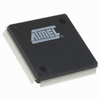
AT91SAM9260B-QU Atmel, AT91SAM9260B-QU Datasheet - Page 584

AT91SAM9260B-QU
Manufacturer Part Number
AT91SAM9260B-QU
Description
IC ARM9 MCU 208-PQFP
Manufacturer
Atmel
Series
AT91SAMr
Specifications of AT91SAM9260B-QU
Core Processor
ARM9
Core Size
16/32-Bit
Speed
180MHz
Connectivity
EBI/EMI, Ethernet, I²C, MMC, SPI, SSC, UART/USART, USB
Peripherals
POR, WDT
Number Of I /o
96
Program Memory Size
32KB (32K x 8)
Program Memory Type
ROM
Ram Size
24K x 8
Voltage - Supply (vcc/vdd)
1.65 V ~ 1.95 V
Data Converters
A/D 4x10b
Oscillator Type
Internal
Operating Temperature
-40°C ~ 85°C
Package / Case
208-MQFP, 208-PQFP
Package
208PQFP
Device Core
ARM926EJ-S
Family Name
91S
Maximum Speed
180 MHz
Operating Supply Voltage
1.8|3.3 V
Data Bus Width
32 Bit
Number Of Programmable I/os
96
Interface Type
EBI/Ethernet/SPI/TWI/UART/USART/USB
On-chip Adc
4-chx10-bit
Number Of Timers
6
Processor Series
AT91SAMx
Core
ARM926EJ-S
Data Ram Size
8 KB
Maximum Clock Frequency
180 MHz
Maximum Operating Temperature
+ 85 C
Mounting Style
SMD/SMT
3rd Party Development Tools
JTRACE-ARM-2M, MDK-ARM, RL-ARM, ULINK2
Development Tools By Supplier
AT91SAM-ICE, AT91-ISP, AT91SAM9260-EK
Minimum Operating Temperature
- 40 C
Cpu Family
AT91
Device Core Size
32b
Frequency (max)
180MHz
Total Internal Ram Size
8KB
# I/os (max)
96
Number Of Timers - General Purpose
6
Operating Supply Voltage (typ)
1.8/3.3V
Operating Supply Voltage (max)
1.95/3.6V
Operating Supply Voltage (min)
1.65/3V
Instruction Set Architecture
RISC
Operating Temp Range
-40C to 85C
Operating Temperature Classification
Industrial
Mounting
Surface Mount
Pin Count
208
Package Type
PQFP
For Use With
AT91SAM9260-EK - KIT EVAL FOR AT91SAM9260AT91SAM-ICE - EMULATOR FOR AT91 ARM7/ARM9
Lead Free Status / RoHS Status
Lead free / RoHS Compliant
Eeprom Size
-
Lead Free Status / Rohs Status
Lead free / RoHS Compliant
Available stocks
Company
Part Number
Manufacturer
Quantity
Price
Company:
Part Number:
AT91SAM9260B-QU
Manufacturer:
ATMEL
Quantity:
2 000
Company:
Part Number:
AT91SAM9260B-QU
Manufacturer:
ATMEL
Quantity:
9
Part Number:
AT91SAM9260B-QU
Manufacturer:
AT
Quantity:
20 000
- Current page: 584 of 798
- Download datasheet (12Mb)
35.4.1.1
35.4.1.2
Table 35-1.
584
Bit
31:2
31
30
29
28
27
1
0
AT91SAM9260
Address of beginning of buffer
Wrap - marks last descriptor in receive buffer descriptor list.
Ownership - needs to be zero for the EMAC to write data to the receive buffer. The EMAC sets this to one once it has
successfully written a frame to memory.
Software has to clear this bit before the buffer can be used again.
Global all ones broadcast address detected
Multicast hash match
Unicast hash match
External address match
Reserved for future use
FIFO
Receive Buffers
Receive Buffer Descriptor Entry
The FIFO depths are
ory latency and network speed.
Data is typically transferred into and out of the FIFOs in bursts of four words. For receive, a bus
request is asserted when the FIFO contains four words and has space for three more. For trans-
mit, a bus request is generated when there is space for four words, or when there is space for
two words if the next transfer is to be only one or two words.
Thus the bus latency must be less than the time it takes to load the FIFO and transmit or receive
three words (12 bytes) of data.
At 100 Mbit/s, it takes 960 ns to transmit or receive 12 bytes of data. In addition, six master clock
cycles should be allowed for data to be loaded from the bus and to propagate through the
FIFOs. For a 60 MHz master clock this takes 100 ns, making the bus latency requirement 860
ns.
Received frames, including CRC/FCS optionally, are written to receive buffers stored in mem-
ory. Each receive buffer is 128 bytes long. The start location for each receive buffer is stored in
memory in a list of receive buffer descriptors at a location pointed to by the receive buffer queue
pointer register. The receive buffer start location is a word address. For the first buffer of a
frame, the start location can be offset by up to three bytes depending on the value written to bits
14 and 15 of the network configuration register. If the start location of the buffer is offset the
available length of the first buffer of a frame is reduced by the corresponding number of bytes.
Each list entry consists of two words, the first being the address of the receive buffer and the
second being the receive status. If the length of a receive frame exceeds the buffer length, the
status word for the used buffer is written with zeroes except for the “start of frame” bit and the
offset bits, if appropriate. Bit zero of the address field is written to one to show the buffer has
been used. The receive buffer manager then reads the location of the next receive buffer and
fills that with receive frame data. The final buffer descriptor status word contains the complete
frame status. Refer to
28
Table 35-1
bytes and
Word 0
Word 1
for details of the receive buffer descriptor list.
28
Function
bytes and area function of the system clock speed, mem-
6221I–ATARM–17-Jul-09
Related parts for AT91SAM9260B-QU
Image
Part Number
Description
Manufacturer
Datasheet
Request
R

Part Number:
Description:
MCU, MPU & DSP Development Tools KICKSTART KIT FOR AT91SAM9 PLUS
Manufacturer:
IAR Systems

Part Number:
Description:
DEV KIT FOR AVR/AVR32
Manufacturer:
Atmel
Datasheet:

Part Number:
Description:
INTERVAL AND WIPE/WASH WIPER CONTROL IC WITH DELAY
Manufacturer:
ATMEL Corporation
Datasheet:

Part Number:
Description:
Low-Voltage Voice-Switched IC for Hands-Free Operation
Manufacturer:
ATMEL Corporation
Datasheet:

Part Number:
Description:
MONOLITHIC INTEGRATED FEATUREPHONE CIRCUIT
Manufacturer:
ATMEL Corporation
Datasheet:

Part Number:
Description:
AM-FM Receiver IC U4255BM-M
Manufacturer:
ATMEL Corporation
Datasheet:

Part Number:
Description:
Monolithic Integrated Feature Phone Circuit
Manufacturer:
ATMEL Corporation
Datasheet:

Part Number:
Description:
Multistandard Video-IF and Quasi Parallel Sound Processing
Manufacturer:
ATMEL Corporation
Datasheet:

Part Number:
Description:
High-performance EE PLD
Manufacturer:
ATMEL Corporation
Datasheet:

Part Number:
Description:
8-bit Flash Microcontroller
Manufacturer:
ATMEL Corporation
Datasheet:

Part Number:
Description:
2-Wire Serial EEPROM
Manufacturer:
ATMEL Corporation
Datasheet:


