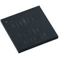
PIC18F67K22-I/MRRSL Microchip Technology, PIC18F67K22-I/MRRSL Datasheet - Page 276

PIC18F67K22-I/MRRSL
Manufacturer Part Number
PIC18F67K22-I/MRRSL
Description
MCU PIC 128K FLASH XLP 64QFN
Manufacturer
Microchip Technology
Series
PIC® XLP™ 18Fr
Datasheets
1.PIC16F722-ISS.pdf
(8 pages)
2.PIC18F65K22T-IPTRSL.pdf
(548 pages)
3.PIC18F65K22T-IPTRSL.pdf
(10 pages)
Specifications of PIC18F67K22-I/MRRSL
Core Size
8-Bit
Program Memory Size
128KB (64K x 16)
Core Processor
PIC
Speed
64MHz
Connectivity
I²C, LIN, SPI, UART/USART
Peripherals
Brown-out Detect/Reset, LVD, POR, PWM, WDT
Number Of I /o
53
Program Memory Type
FLASH
Eeprom Size
1K x 8
Ram Size
4K x 8
Voltage - Supply (vcc/vdd)
1.8 V ~ 5.5 V
Data Converters
A/D 16x12b
Oscillator Type
Internal
Operating Temperature
-40°C ~ 85°C
Package / Case
64-VFQFN, Exposed Pad
Controller Family/series
PIC18
Eeprom Memory Size
1024Byte
Ram Memory Size
3862Byte
Cpu Speed
16MIPS
No. Of Timers
11
Processor Series
PIC18F
Core
PIC
Data Bus Width
8 bit
Data Ram Size
4 KB
Interface Type
I2C, SPI, EUSART
Maximum Clock Frequency
64 MHz
Number Of Programmable I/os
53
Number Of Timers
11
Operating Supply Voltage
1.8 V to 5.5 V
Maximum Operating Temperature
+ 85 C
Mounting Style
SMD/SMT
3rd Party Development Tools
52715-96, 52716-328, 52717-734, 52712-325, EWPIC18
Development Tools By Supplier
DM180021, DM183026-2, DM183032, DV164131, MA180028
Minimum Operating Temperature
- 40 C
On-chip Adc
12 bit, 16 Channel
Lead Free Status / RoHS Status
Lead free / RoHS Compliant
Lead Free Status / RoHS Status
Lead free / RoHS Compliant
Available stocks
Company
Part Number
Manufacturer
Quantity
Price
Company:
Part Number:
PIC18F67K22-I/MRRSL
Manufacturer:
FSC
Quantity:
250
- PIC16F722-ISS PDF datasheet
- PIC18F65K22T-IPTRSL PDF datasheet #2
- PIC18F65K22T-IPTRSL PDF datasheet #3
- Current page: 276 of 548
- Download datasheet (5Mb)
PIC18F87K22 FAMILY
FIGURE 20-16:
FIGURE 20-17:
FIGURE 20-18:
DS39960B-page 276
Note 1: Port outputs are configured as displayed when
P1<D:A>
PORT Data
PORT Data
PORT Data
PORT Data
STRn
P1<D:A>
PxA Signal
PWM
CCPxM1
CCPxM0
CCPxM1
CCPxM0
2: Single PWM output requires setting at least
STRn
PWM
STRA
STRB
STRC
STRD
the CCPxCON register bits, PxM<1:0> = 00
and CCP1M<3:2> = 11.
one of the STRx bits.
PORT Data
SIMPLIFIED STEERING
BLOCK DIAGRAM
EXAMPLE OF STEERING EVENT AT END OF INSTRUCTION (STRSYNC = 0)
EXAMPLE OF STEERING EVENT AT BEGINNING OF INSTRUCTION (STRSYNC = 1)
1
0
1
0
1
0
1
0
PORT Data
PWM Period
TRIS
TRIS
TRIS
TRIS
Output Pin
Output Pin
Output Pin
Output Pin
Preliminary
P1n = PWM
20.4.7.1
The STRSYNC bit of the PSTRxCON register gives the
user two choices for when the steering event will
happen. When the STRSYNC bit is ‘0’, the steering
event will happen at the end of the instruction that
writes to the PSTRxCON register. In this case, the out-
put signal at the Px<D:A> pins may be an incomplete
PWM waveform. This operation is useful when the user
firmware needs to immediately remove a PWM signal
from the pin.
When the STRSYNC bit is ‘1’, the effective steering
update will happen at the beginning of the next PWM
period. In this case, steering on/off the PWM output will
always produce a complete PWM waveform.
Figures 20-17 and 20-18 illustrate the timing diagrams
of the PWM steering depending on the STRSYNC
setting.
P1n = PWM
Steering Synchronization
PORT Data
2010 Microchip Technology Inc.
PORT Data
Related parts for PIC18F67K22-I/MRRSL
Image
Part Number
Description
Manufacturer
Datasheet
Request
R

Part Number:
Description:
MCU PIC 128K FLASH XLP 64TQFP
Manufacturer:
Microchip Technology
Datasheet:

Part Number:
Description:
128kB Flash, 4kB RAM, 1kB EE, NanoWatt XLP, GP 64 QFN 9x9x0.9mm TUBE
Manufacturer:
Microchip Technology
Datasheet:

Part Number:
Description:
128kB Flash, 4kB RAM, 1kB EE, NanoWatt XLP, GP 64 TQFP 10x10x1mm TRAY
Manufacturer:
Microchip Technology
Datasheet:

Part Number:
Description:
128kB Flash, 4kB RAM, 1kB EE, NanoWatt XLP, GP 64 QFN 9x9x0.9mm TUBE
Manufacturer:
Microchip Technology
Datasheet:

Part Number:
Description:
128kB Flash, 4kB RAM, 1kB EE, NanoWatt XLP, GP 64 TQFP 10x10x1mm TRAY
Manufacturer:
Microchip Technology

Part Number:
Description:
Manufacturer:
Microchip Technology Inc.
Datasheet:

Part Number:
Description:
Manufacturer:
Microchip Technology Inc.
Datasheet:

Part Number:
Description:
Manufacturer:
Microchip Technology Inc.
Datasheet:

Part Number:
Description:
Manufacturer:
Microchip Technology Inc.
Datasheet:

Part Number:
Description:
Manufacturer:
Microchip Technology Inc.
Datasheet:

Part Number:
Description:
Manufacturer:
Microchip Technology Inc.
Datasheet:


