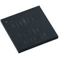
PIC18F67K22-I/MRRSL Microchip Technology, PIC18F67K22-I/MRRSL Datasheet - Page 116

PIC18F67K22-I/MRRSL
Manufacturer Part Number
PIC18F67K22-I/MRRSL
Description
MCU PIC 128K FLASH XLP 64QFN
Manufacturer
Microchip Technology
Series
PIC® XLP™ 18Fr
Datasheets
1.PIC16F722-ISS.pdf
(8 pages)
2.PIC18F65K22T-IPTRSL.pdf
(548 pages)
3.PIC18F65K22T-IPTRSL.pdf
(10 pages)
Specifications of PIC18F67K22-I/MRRSL
Core Size
8-Bit
Program Memory Size
128KB (64K x 16)
Core Processor
PIC
Speed
64MHz
Connectivity
I²C, LIN, SPI, UART/USART
Peripherals
Brown-out Detect/Reset, LVD, POR, PWM, WDT
Number Of I /o
53
Program Memory Type
FLASH
Eeprom Size
1K x 8
Ram Size
4K x 8
Voltage - Supply (vcc/vdd)
1.8 V ~ 5.5 V
Data Converters
A/D 16x12b
Oscillator Type
Internal
Operating Temperature
-40°C ~ 85°C
Package / Case
64-VFQFN, Exposed Pad
Controller Family/series
PIC18
Eeprom Memory Size
1024Byte
Ram Memory Size
3862Byte
Cpu Speed
16MIPS
No. Of Timers
11
Processor Series
PIC18F
Core
PIC
Data Bus Width
8 bit
Data Ram Size
4 KB
Interface Type
I2C, SPI, EUSART
Maximum Clock Frequency
64 MHz
Number Of Programmable I/os
53
Number Of Timers
11
Operating Supply Voltage
1.8 V to 5.5 V
Maximum Operating Temperature
+ 85 C
Mounting Style
SMD/SMT
3rd Party Development Tools
52715-96, 52716-328, 52717-734, 52712-325, EWPIC18
Development Tools By Supplier
DM180021, DM183026-2, DM183032, DV164131, MA180028
Minimum Operating Temperature
- 40 C
On-chip Adc
12 bit, 16 Channel
Lead Free Status / RoHS Status
Lead free / RoHS Compliant
Lead Free Status / RoHS Status
Lead free / RoHS Compliant
Available stocks
Company
Part Number
Manufacturer
Quantity
Price
Company:
Part Number:
PIC18F67K22-I/MRRSL
Manufacturer:
FSC
Quantity:
250
- PIC16F722-ISS PDF datasheet
- PIC18F65K22T-IPTRSL PDF datasheet #2
- PIC18F65K22T-IPTRSL PDF datasheet #3
- Current page: 116 of 548
- Download datasheet (5Mb)
PIC18F87K22 FAMILY
7.5.1
The sequence of events for programming an internal
program memory location should be:
1.
2.
3.
4.
5.
6.
7.
8.
9.
10. Write 0xAA to EECON2.
11. Set the WR bit. This will begin the write cycle.
12. Re-enable the interrupts.
13. Verify the memory (table read).
DS39960B-page 116
Read the 64 or 128 bytes into RAM.
Update the data values in RAM as necessary.
Load the Table Pointer register with the address
being erased.
Execute the row erase procedure.
Load the Table Pointer register with the address
of the first byte being written.
Write the 64 or 128 bytes into the holding
registers with auto-increment.
Set the EECON1 register for the write operation:
• Set the EEPGD bit to point to program memory
• Clear the CFGS bit to access program memory
• Set the WREN to enable byte writes
Disable the interrupts.
Write 0x55 to EECON2.
The CPU will stall for duration of the write for T
(see parameter D133A).
FLASH PROGRAM MEMORY WRITE
SEQUENCE
IW
Preliminary
An example of the required code is shown in
Example 7-3 on the following page.
Note:
Note:
Before setting the WR bit, the Table
Pointer address needs to be within the
intended address range of the 64 or
128 bytes in the holding register.
Self-write
EEPROM memory cannot be done while
running in LP Oscillator mode (Low-Power
mode). Therefore, executing a self-write
will put the device into High-Power mode.
2010 Microchip Technology Inc.
execution
to
Flash
and
Related parts for PIC18F67K22-I/MRRSL
Image
Part Number
Description
Manufacturer
Datasheet
Request
R

Part Number:
Description:
MCU PIC 128K FLASH XLP 64TQFP
Manufacturer:
Microchip Technology
Datasheet:

Part Number:
Description:
128kB Flash, 4kB RAM, 1kB EE, NanoWatt XLP, GP 64 QFN 9x9x0.9mm TUBE
Manufacturer:
Microchip Technology
Datasheet:

Part Number:
Description:
128kB Flash, 4kB RAM, 1kB EE, NanoWatt XLP, GP 64 TQFP 10x10x1mm TRAY
Manufacturer:
Microchip Technology
Datasheet:

Part Number:
Description:
128kB Flash, 4kB RAM, 1kB EE, NanoWatt XLP, GP 64 QFN 9x9x0.9mm TUBE
Manufacturer:
Microchip Technology
Datasheet:

Part Number:
Description:
128kB Flash, 4kB RAM, 1kB EE, NanoWatt XLP, GP 64 TQFP 10x10x1mm TRAY
Manufacturer:
Microchip Technology

Part Number:
Description:
Manufacturer:
Microchip Technology Inc.
Datasheet:

Part Number:
Description:
Manufacturer:
Microchip Technology Inc.
Datasheet:

Part Number:
Description:
Manufacturer:
Microchip Technology Inc.
Datasheet:

Part Number:
Description:
Manufacturer:
Microchip Technology Inc.
Datasheet:

Part Number:
Description:
Manufacturer:
Microchip Technology Inc.
Datasheet:

Part Number:
Description:
Manufacturer:
Microchip Technology Inc.
Datasheet:


