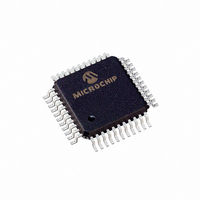
PIC16LC65B-04/PQ Microchip Technology, PIC16LC65B-04/PQ Datasheet - Page 81

PIC16LC65B-04/PQ
Manufacturer Part Number
PIC16LC65B-04/PQ
Description
IC MCU OTP 4KX14 PWM 44-MQFP
Manufacturer
Microchip Technology
Series
PIC® 16Cr
Specifications of PIC16LC65B-04/PQ
Core Processor
PIC
Core Size
8-Bit
Speed
4MHz
Connectivity
I²C, SPI, UART/USART
Peripherals
Brown-out Detect/Reset, POR, PWM, WDT
Number Of I /o
33
Program Memory Size
7KB (4K x 14)
Program Memory Type
OTP
Ram Size
192 x 8
Voltage - Supply (vcc/vdd)
2.5 V ~ 5.5 V
Oscillator Type
External
Operating Temperature
0°C ~ 70°C
Package / Case
44-MQFP, 44-PQFP
Processor Series
PIC16LC
Core
PIC
Data Bus Width
8 bit
Data Ram Size
192 B
Interface Type
I2C, SPI, USART
Maximum Clock Frequency
20 MHz
Number Of Programmable I/os
33
Number Of Timers
3
Operating Supply Voltage
2.5 V to 6 V
Maximum Operating Temperature
+ 70 C
Mounting Style
SMD/SMT
3rd Party Development Tools
52715-96, 52716-328, 52717-734
Development Tools By Supplier
ICE2000, DM163022
Minimum Operating Temperature
0 C
Data Rom Size
192 B
Height
2 mm
Length
10 mm
Supply Voltage (max)
5.5 V
Supply Voltage (min)
3.65 V
Width
10 mm
Lead Free Status / RoHS Status
Lead free / RoHS Compliant
Eeprom Size
-
Data Converters
-
Lead Free Status / Rohs Status
Details
Available stocks
Company
Part Number
Manufacturer
Quantity
Price
Company:
Part Number:
PIC16LC65B-04/PQ
Manufacturer:
SIGMADESI
Quantity:
400
Company:
Part Number:
PIC16LC65B-04/PQ
Manufacturer:
Microchip Technology
Quantity:
10 000
The following steps should be followed for doing an A/D
conversion:
1.
2.
FIGURE 12-1:
2000 Microchip Technology Inc.
Note 1: Not available on PIC16C73B.
Configure the A/D module:
• Configure analog pins, voltage reference,
• Select A/D input channel (ADCON0)
• Select A/D conversion clock (ADCON0)
• Turn on A/D module (ADCON0)
Configure A/D interrupt (if desired):
• Clear ADIF bit (PIR1<6>)
• Set ADIE bit (PIE1<6>)
• Set PEIE bit (INTCON<6>)
• Set GIE bit (INTCON<7>)
and digital I/O (ADCON1)
Converter
A/D
A/D BLOCK DIAGRAM
(Reference
Voltage)
V
REF
(Input Voltage)
PCFG2:PCFG0
V
IN
PIC16C63A/65B/73B/74B
V
DD
001 or
011 or
101
000 or
010 or
100 or
11x
3.
4.
5.
6.
7.
Wait the required acquisition time.
Set GO/DONE bit (ADCON0) to start conversion.
Wait for A/D conversion to complete, by either:
Polling for the GO/DONE bit to be cleared (if
interrupts are disabled);
OR
Waiting for the A/D interrupt.
Read A/D result register (ADRES), clear bit
ADIF if required.
For next conversion, go to step 1 or step 2 as
required. The A/D conversion time per bit is
defined as T
required before next acquisition starts.
CHS2:CHS0
111
110
101
100
011
010
001
000
AD
. A minimum wait of 2 T
RA1/AN1
RE2/AN7
RA2/AN2
RA0/AN0
RE1/AN6
RE0/AN5
RA5/AN4
RA3/AN3/V
DS30605C-page 81
(1)
(1)
(1)
REF
AD
is


