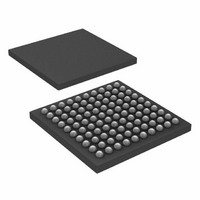
ATXMEGA64A1-C7U Atmel, ATXMEGA64A1-C7U Datasheet - Page 101

ATXMEGA64A1-C7U
Manufacturer Part Number
ATXMEGA64A1-C7U
Description
IC MCU AVR 64KB FLASH 100VFBGA
Manufacturer
Atmel
Series
AVR® XMEGAr
Datasheet
1.ATAVRONEKIT.pdf
(113 pages)
Specifications of ATXMEGA64A1-C7U
Core Processor
AVR
Core Size
8/16-Bit
Speed
32MHz
Connectivity
EBI/EMI, I²C, IrDA, SPI, UART/USART
Peripherals
Brown-out Detect/Reset, DMA, POR, PWM, WDT
Number Of I /o
78
Program Memory Size
64KB (32K x 16)
Program Memory Type
FLASH
Eeprom Size
2K x 8
Ram Size
4K x 8
Voltage - Supply (vcc/vdd)
1.6 V ~ 3.6 V
Data Converters
A/D 16x12b, D/A 4x12b
Oscillator Type
Internal
Operating Temperature
-40°C ~ 85°C
Package / Case
100-VFBGA
Processor Series
XMEGA
Core
AVR
Data Bus Width
8 bit, 16 bit
Data Ram Size
4 KB
Interface Type
SPI, TWI, USART
Maximum Clock Frequency
32 MHz
Number Of Programmable I/os
78
Number Of Timers
8
Operating Supply Voltage
2.5 V
Maximum Operating Temperature
+ 85 C
Mounting Style
SMD/SMT
3rd Party Development Tools
EWAVR, EWAVR-BL
Development Tools By Supplier
ATAVRDRAGON, ATAVRISP2, ATAVRONEKIT
Minimum Operating Temperature
- 40 C
Operating Temperature Range
- 40 C to + 85 C
Lead Free Status / RoHS Status
Lead free / RoHS Compliant
Available stocks
Company
Part Number
Manufacturer
Quantity
Price
8067M–AVR–09/10
4. ADC gain stage output range is limited to 2.4 V
5. The ADC has up to ±2 LSB inaccuracy
6. TWI, a general address call will match independent of the R/W-bit value
7. TWI, the minimum I
8. Setting HIRES PR bit makes PWM output unavailable
The amplified output of the ADC gain stage will never go above 2.4 V, hence the differential
input will only give correct output when below 2.4 V/gain. For the available gain settings, this
gives a differential input range of:
Problem fix/Workaround
Keep the amplified voltage output from the ADC gain stage below 2.4 V in order to get a cor-
rect result, or keep ADC voltage reference below 2.4 V.
The ADC will have up to ±2 LSB inaccuracy, visible as a saw-tooth pattern on the input volt-
age/ output value transfer function of the ADC. The inaccuracy increases with increasing
voltage reference reaching ±2 LSB with 3V reference.
Problem fix/Workaround
None, the actual ADC resolution will be reduced with up to ±2 LSB.
When the TWI is in Slave mode and a general address call is issued on the bus, the TWI
Slave will get an address match regardless of the R/W-bit (ADDR[0] bit) value in the Slave
Address Register.
Problem fix/Workaround
Use software to check the R/W-bit on general call address match.
When the TWI is in Master Read mode and issuing a Repeated Start on the bus, this will
immediately release the SCL line even if one complete SCL low period has not passed. This
means that the minimum SCL low time in the I
Problem fix/Workaround
If this causes a potential problem in the application, software must ensure that the Repeated
Start is never issued before one SCL low time has passed.
Setting the HIRES Power Reduction (PR) bit for PORTx will make any Frequency or PWM
output for the corresponding Timer/Counters (TCx0 and TCx1) unavailable on the pin.
Problem fix/Workaround
Do not write the HIRES PR bit on PORTx when frequency or PWM output from TCx0/1 is
used.
–
–
–
–
–
–
–
16x
32x
64x
1x
2x
4x
8x
gain:
gain:
gain:
gain:
gain:
gain:
gain:
300
150
2
2.4
1.2
0.6
75
38
C SCL low time could be violated in Master Read mode
V
V
V
mV
mV
mV
mV
2
C specification could be violated.
XMEGA A1
101


