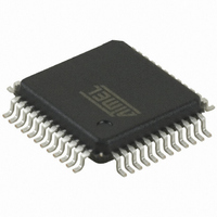
AT32UC3L064-AUR Atmel, AT32UC3L064-AUR Datasheet - Page 15

AT32UC3L064-AUR
Manufacturer Part Number
AT32UC3L064-AUR
Description
IC MCU AVR32 64K FLASH 48TQFP
Manufacturer
Atmel
Series
AVR®32 UC3r
Datasheet
1.AT32UC3L016-ZAUR.pdf
(71 pages)
Specifications of AT32UC3L064-AUR
Package / Case
48-TQFP, 48-VQFP
Voltage - Supply (vcc/vdd)
1.62 V ~ 1.98 V
Operating Temperature
-40°C ~ 85°C
Speed
50MHz
Number Of I /o
36
Core Processor
AVR
Program Memory Type
FLASH
Ram Size
16K x 8
Program Memory Size
64KB (64K x 8)
Data Converters
A/D 9x10b
Oscillator Type
Internal
Peripherals
Brown-out Detect/Reset, DMA, PWM, WDT
Connectivity
I²C, SPI, UART/USART
Core Size
32-Bit
Lead Free Status / RoHS Status
Lead free / RoHS Compliant
Eeprom Size
-
Available stocks
Company
Part Number
Manufacturer
Quantity
Price
Company:
Part Number:
AT32UC3L064-AUR
Manufacturer:
ATMEL
Quantity:
101
3.4
3.4.1
3.4.2
3.4.3
3.4.4
3.4.5
3.5
3.5.1
32099AS–AVR32–06/09
I/O Line Considerations
Power Considerations
JTAG Pins
RESET_N Pin
TWI Pins
GPIO Pins
ADC Input Pins
Power Supplies
The JTAG is enabled if TCK is low while the RESET_N pin is released. The TCK, TMS, and TDI
pins have pull-up resistors when JTAG is enabled. TDO pin is an output, driven at VDDIO, and
has no pull-up resistor. These JTAG pins can be used as GPIO pins and muxed with peripherals
when the JTAG is disabled.
The RESET_N pin is a schmitt input and integrates a permanent pull-up resistor to VDDIO. As
the product integrates a power-on reset detector, the RESET_N pin can be left unconnected in
case no reset from the system needs to be applied to the product.
The RESET_N pin is also used for the aWire debug protocol. When the pin is used for debug-
ging, it must not be driven by the application.
When these pins are used for TWI, the pins are open-drain outputs with slew-rate limitation and
inputs with inputs with spike-filtering. When used as GPIO pins or used for other peripherals, the
pins have the same characteristics as GPIO pins.
All the I/O lines integrate a pull-up resistor. Programming of this pull-up resistor is performed
independently for each I/O line through the GPIO Controllers. After reset, I/O lines default as
inputs with pull-up resistors disabled, except PA00.
These pins are regular I/O pins powered from the VDDIO. However, when these pins are used
for ADC inputs, the voltage applied to the pin must not exceed 1.98V. Internal circuitry ensures
that the pin cannot be used as an analog input pin when the I/O drives to VDD. When the pins
are not used for ADC inputs, the pins may be driven to the full I/O voltage range.
The AT32UC3L has several types of power supply pins:
• VDDIO: Powers I/O lines. Voltage is 1.8 to 3.3V nominal.
• VDDIN: Powers I/O lines and the internal regulator. Voltage is 1.8 to 3.3V nominal.
• VDDANA: Powers the ADC. Voltage is 1.8V nominal.
• VDDCORE: Powers the core, memories, and peripherals. Voltage is 1.8V nominal.
The ground pins GND are common to VDDCORE and VDDIO. The ground pin for VDDANA is
GNDANA.
Refer to
pins.
”Electrical Characteristics” on page 40
for power consumption on the various supply
AT32UC3L
15


