AT32UC3L064-AUR Atmel, AT32UC3L064-AUR Datasheet
AT32UC3L064-AUR
Specifications of AT32UC3L064-AUR
Available stocks


Related parts for AT32UC3L064-AUR


AT32UC3L064-AUR Summary of contents
Page 1
... SPI Slaves can be Addressed • Two Master and Two Slave Two-Wire Interfaces (TWI), 400kbit/s I • One 9-channel Analog-To-Digital Converter (ADC) with Bits Resolution – Internal Temperature Sensor ® 32-bit Microcontroller 2 C-compatible ® AVR 32 32-bit Microcontroller AT32UC3L064 AT32UC3L032 AT32UC3L016 Preliminary Summary 32099AS–AVR32–06/09 ...
Page 2
Eight Analog Comparators (AC) with Optional Window Detection • Capacitive Touch (CAT) Module ™ – Support QTouch and QMatrix • On-Chip Non-Intrusive Debug System – Nexus Class 2+, Runtime Control, Non-Intrusive Data and Program Trace ™ – aWire Single-Pin ...
Page 3
Description The AT32UC3L is a complete System-On-Chip microcontroller based on the AVR32 UC RISC processor running at frequencies up to 50MHz. AVR32 high-performance 32-bit RISC microprocessor core, designed for cost-sensitive embedded applications, with particular empha- sis ...
Page 4
The Pulse Width Modulation controller (PWMA) provides 8-bit PWM channels which can be syn- chronized and controlled from a common timer. One PWM channel is available for each I/O pin on the device, enabling applications that require multiple PWM outputs, ...
Page 5
Overview 2.1 Block Diagram Figure 2-1. RESET_N PA PB 32099AS–AVR32–06/09 Block Diagram MCKO MDO[5..0] MSEO[1..0] EVTI_N NEXUS EVTO_N CLASS 2+ TCK MEMORY PROTECTION UNIT JTAG OCD TDO INTERFACE TDI INSTR TMS INTERFACE aWire M HIGH SPEED BUS MATRIX S ...
Page 6
Configuration Summary Table 2-1. Feature Flash SRAM GPIO Hi-drive pins External Interrupts TWI USART Peripheral DMA Channels Peripheral Event System SPI Asynchronous Timers Timer/Counter Channels PWM channels Frequency Meter Watchdog Timer Power Manager Oscillators ADC Temperature Sensor Analog Comparators ...
Page 7
Package and Pinout 3.1 Package The device pins are multiplexed with peripheral functions as described in Figure 3-1. PA15 PA16 PA17 PA19 PA18 VDDIO GND PB11 GND PA10 PA12 VDDIO 3.2 Peripheral Multiplexing on I/O lines 3.2.1 Multiplexed signals ...
Page 8
Table 3-1. GPIO Controller Function Multiplexing Pad 48 PIN O Supply Type Normal 11 PA00 0 VDDIO I/O Normal 14 PA01 1 VDDIO I/O High- 13 PA02 2 VDDIO drive I/O Normal 4 PA03 3 ...
Page 9
Table 3-1. GPIO Controller Function Multiplexing TWI, 5V tolerant, 24 PA21 21 VDDIN SMBus, Normal I/O Normal 9 PA22 22 VDDIO I/O Normal 6 PB00 32 VDDIO I/O High- 16 PB01 33 VDDIO drive I/O Normal 7 PB02 34 VDDIO ...
Page 10
Peripheral Functions Each GPIO line can be assigned to one of several peripheral functions. The following table describes how the various peripheral functions are selected. The last listed function has priority in case multiple functions are enabled. Table 3-2. ...
Page 11
Table 3-4. Pin EVTO_N MCKO MSEO[1] MSEO[0] 3.2.5 Oscillator Pinout The oscillators are not mapped to the normal GPIO functions and their muxings are controlled by registers in the System Control Interface (SCIF). Please refer to the SCIF chapter for ...
Page 12
Signal Descriptions The following table gives details on signal name classified by peripheral. Table 3-7. Signal Descriptions List Signal Name Function ACAN3 - ACAN0 Negative inputs for comparators "A" ACAP3 - ACAP0 Positive inputs for comparators "A" ACBN3 - ...
Page 13
Table 3-7. Signal Descriptions List RESET_N Reset PWMA35 - PWMA0 PWMA channel waveforms PWMAOD35 - PWMA channel waveforms, open drain PWMAOD0 mode GCLK4 - GCLK0 Generic Clock Output RC32OUT RC32K output at startup XIN0 Crystal 0 Input XIN32 Crystal 32 ...
Page 14
Table 3-7. Signal Descriptions List CTS Clear To Send RTS Request To Send RXD Receive Data TXD Transmit Data Table 3-8. Signal Description List, continued Signal Name Function VDDCORE Core Power Supply / Voltage Regulator Output VDDIO I/O Power Supply ...
Page 15
I/O Line Considerations 3.4.1 JTAG Pins The JTAG is enabled if TCK is low while the RESET_N pin is released. The TCK, TMS, and TDI pins have pull-up resistors when JTAG is enabled. TDO pin is an output, driven ...
Page 16
Voltage Regulator The AT32UC3L embeds a voltage regulator that converts from 3.3V nominal to 1.8V with a load mA. The regulator supplies the output voltage on VDDCORE. VDDCORE should be externally connected to the 1.8V ...
Page 17
Figure 3-3. TBD-3.6V VDDCORE VDDANA 32099AS–AVR32–06/09 3.3V Single Power Supply mode + - VDDIN I/O Pins Linear ADC GNDANA AT32UC3L VDDIO GND I/O Pins OSC32K RC32K AST Wake POR33 SM33 CPU, Peripherals, Memories, SCIF, BOD, RCSYS, DFLL 17 ...
Page 18
Single Supply Mode In 1.8V single supply mode the internal regulator is not used, and VDDIO and VDDCORE are powered by a single 1.8V supply as shown in same power (VDDIN = VDDIO = VDDCORE). Figure 3-4. 1.62-1.98V ...
Page 19
Supply Mode with 1.8V Regulated I/O Lines In this mode, the internal regulator is connected to the 3.3V source and its output is connected to both VDDCORE and VDDIO as shown in use Shutdown mode. Figure 3-5. In ...
Page 20
Power-up Sequence 3.5.4.1 Maximum Rise Rate To avoid risk of latch-up, the rise rate of the power supplies must not exceed the values described in Recommended order for power supplies is also described in this table. 3.5.4.2 Minimum Rise ...
Page 21
Processor and Architecture Rev: 2.1.0.0 This chapter gives an overview of the AVR32UC CPU. AVR32UC is an implementation of the AVR32 architecture. A summary of the programming model, instruction set, and MPU is pre- sented. For further details, see ...
Page 22
The register file is organized as sixteen 32-bit registers and includes the Program Counter, the Link Register, and the Stack Pointer. In addition, register R12 is designed to hold return values from function calls and is used implicitly by some ...
Page 23
Figure 4-1. Instruction memory controller 4.3.1 Pipeline Overview AVR32UC has three pipeline stages, Instruction Fetch (IF), Instruction Decode (ID), and Instruc- tion Execute (EX). The EX stage is split into three parallel subsections, one arithmetic/logic (ALU) section, one multiply (MUL) ...
Page 24
Figure 4-2. 4.3.2 AVR32A Microarchitecture Compliance AVR32UC implements an AVR32A microarchitecture. The AVR32A microarchitecture is tar- geted at cost-sensitive, lower-end applications like smaller microcontrollers. This microarchitecture does not provide dedicated hardware registers for shadowing of register file registers in interrupt ...
Page 25
The following table shows the instructions with support for unaligned addresses. All other instructions require aligned addresses. Table 4-1. Instruction ld.d st.d 4.3.2.5 Unimplemented Instructions The following instructions are unimplemented in AVR32UC, and will cause an Unimplemented Instruction Exception if ...
Page 26
Programming Model 4.4.1 Register File Configuration The AVR32UC register file is shown below. Figure 4-3. Application Bit 31 Bit SP_APP R12 R11 R10 R9 R8 INT0PC R7 INT1PC R6 FINTPC R5 SMPC ...
Page 27
Figure 4-5. Bit 4.4.3 Processor States 4.4.3.1 Normal RISC State The AVR32 processor supports several different execution contexts as shown in Table 4-2. Priority N/A N/A Mode changes can ...
Page 28
Debug state can be entered as described in the AVR32UC Technical Reference Manual. Debug state is exited by the retd instruction. 4.4.3.3 Secure State The AVR32 can be set in a secure state, that allows a part of the code ...
Page 29
Table 4-3. Reg # 33- ...
Page 30
Table 4-3. Reg # 100 101 102 103 104 105 106 107 108 109 110 111 112-191 192-255 4.5 Exceptions and Interrupts In the AVR32 architecture, events are used as ...
Page 31
EVBA. The autovector offset has 14 address bits, giving an offset of maximum 16384 bytes. The target address of the event handler is calculated as (EVBA | event_handler_offset), not (EVBA + event_handler_offset), so EVBA and exception code segments ...
Page 32
Supervisor Calls The AVR32 instruction set provides a supervisor mode call instruction. The scall instruction is designed so that privileged routines can be called from any context. This facilitates sharing of code between different execution modes. The scall mechanism ...
Page 33
An instruction B is younger than an instruction was sent down the pipeline later than A. The addresses and priority of simultaneous events are shown in the exceptions are unused in AVR32UC since ...
Page 34
Table 4-4. Priority and Handler Addresses for Events Priority Handler Address 1 0x80000000 2 Provided by OCD system 3 EVBA+0x00 4 EVBA+0x04 5 EVBA+0x08 6 EVBA+0x0C 7 EVBA+0x10 8 Autovectored 9 Autovectored 10 Autovectored 11 Autovectored 12 EVBA+0x14 13 EVBA+0x50 ...
Page 35
... Internal High-Speed SRAM, Single-cycle access at full speed – 16Kbytes (AT32UC3L064, AT32UC3L032) – 8Kbytes (AT32UC3L016) 5.2 Physical Memory Map The system bus is implemented as a bus matrix. All system bus addresses are fixed, and they are never remapped in any way, not even in boot ...
Page 36
Peripheral Address Map Table 5-3. Peripheral Address Mapping Address 0xFFFE0000 0xFFFE0400 0xFFFE0800 0xFFFF0000 0xFFFF1000 0xFFFF1400 0xFFFF1800 0xFFFF1C00 0xFFFF2000 0xFFFF2400 0xFFFF2800 0xFFFF2C00 0xFFFF3000 0xFFFF3400 0xFFFF3800 0xFFFF3C00 0xFFFF4000 0xFFFF4400 32099AS–AVR32–06/09 Peripheral Name FLASHCDW Flash Controller - FLASHCDW HMATRIX HSB Matrix - ...
Page 37
Table 5-3. Peripheral Address Mapping 0xFFFF4800 0xFFFF4C00 0xFFFF5000 0xFFFF5400 0xFFFF5800 0xFFFF5C00 0xFFFF6000 0xFFFF6400 0xFFFF6800 0xFFFF6C00 0xFFFF7000 5.4 CPU Local Bus Mapping Some of the registers in the GPIO module are mapped onto the CPU local bus, in addition to being ...
Page 38
The following GPIO registers are mapped on the local bus: Table 5-4. Port A B 32099AS–AVR32–06/09 Local Bus Mapped GPIO Registers Register Output Driver Enable Register (ODER) Output Value Register (OVR) Pin Value Register (PVR) Output Driver Enable Register (ODER) ...
Page 39
Boot Sequence This chapter summarizes the boot sequence of the AT32UC3L. The behavior after power-up is controlled by the Power Manager. For specific details, refer to the Power Manager chapter. 6.1 Starting of Clocks After power-up, the device will ...
Page 40
Electrical Characteristics 7.1 Disclaimer All values in this chapter are preliminary and subject to change without further notice. 7.2 Absolute Maximum Ratings* Table 7-1. Absolute Maximum Ratings Operating temperature..................................... -40°C to +85°C Storage temperature...................................... -60°C to +150°C Voltage on ...
Page 41
Table 7-3. Symbol V VDDIO V VDDIN V VDDCORE V VDDANA Note: 7.4 Clock Characteristics These parameters are given in the following conditions: V VDDCORE Temperature = -40°C to 85°C Table 7-4. Symbol f CPU f PBA f PBB 7.5 ...
Page 42
Figure 7-1. Table 7-5. Power Consumption for Different Modes Mode Conditions Active Active mode (2) Idle Idle Frozen Frozen sleep mode Standby Standby sleep mode Stop Stop sleep mode DeepStop DeepStop sleep mode Static sleep mode with Static (4) RTC ...
Page 43
Table 7-6. Peripheral ACIFB ADCIFB AST AW CAT EIC FLASHCDW FREQM GPIO HMATRIX INTC PDCA PM PWMA SAU SCIF SPI TC TWIM TWIS USART WDT 32099AS–AVR32–06/09 Power Consumption by Peripheral in Active Mode AT32UC3L Consumption Typ Unit TBD TBD TBD ...
Page 44
I/O Pad Characteristics Table 7-7. Normal I/O Pad Characteristics Symbol Parameter R Pull-up resistance PULLUP V Input low-level voltage IL V Input high-level voltage IH V Output low-level voltage OL V Output high-level voltage OH I Output low-level current ...
Page 45
Table 7-9. 5V Tolerant I/O Pad Characteristics Symbol Parameter I Output High-level Current OH I Input Leakage Current LEAK C Input Capacitance IN Table 7-10. TWI Pad Characteristics Symbol Parameter R Pull-up Resistance PULLUP V Input Low-level Voltage IL V ...
Page 46
Table 7-12. Oscillator I/O Pad Characteristics Symbol Parameter V Output Low-level Voltage OL V Output High-level Voltage OH I Output Low-level Current OL I Output High-level Current OH I Input Leakage Current LEAK C Input Capacitance IN 7.7 Oscillator Characteristics ...
Page 47
KHz Crystal Oscillator Characteristics Table 7-16. 32 KHz Crystal Oscillator Characteristics Symbol Parameter 1/(t ) Crystal oscillator frequency CP32KHz t Startup time ST C Equivalent load capacitance L I Current consumption OSC Note the equivalent ...
Page 48
DFLL Characteristics Table 7-17. Digital Frequency Locked Loop Characteristics Symbol Parameter f Output frequency OUT f Input frequency IN I Current consumption DFLL t Startup time STARTUP t Lock time LOCK 7.7.4 RC120M Characteristics Table 7-18. Internal 120MHz RC ...
Page 49
Table 7-21. Maximum Operating Frequency Flash Wait States 7.9 Analog Characteristics 7.9.1 Regulator Characteristics 7.9.1.1 Electrical Characteristics Table 7-22. Electrical Characteristics Symbol Parameter Maximum DC output current with V I OUT Maximum DC output current with ...
Page 50
POR Table 7-24. Power-on Reset Characteristics Symbol Parameter POR threshold voltage (rising) V POT POR threshold voltage (falling) 7.9.3 SM33 Table 7-25. SM33 Characteristics Symbol Parameter V Voltage threshold TH 7.9.4 POR33 Table 7-26. POR33 Characteristics Symbol Parameter V ...
Page 51
Mechanical Characteristics 8.1 Thermal Considerations 8.1.1 Thermal Data Table 8-1 Table 8-1. Symbol θ JA θ JC θ JA θ JC θ JA θ JC 8.1.2 Junction Temperature The average chip-junction temperature where: • ...
Page 52
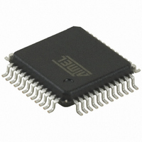
Package Drawings Figure 8-1. TQFP-48 Package Drawing Table 8-2. Device and Package Maximum Weight TBD Table 8-3. Package Characteristics Moisture Sensitivity Level Table 8-4. Package Reference JEDEC Drawing Reference JESD97 Classification 32099AS–AVR32–06/09 mg TBD MS-026 E3 AT32UC3L 52 ...
Page 53
Figure 8-2. QFN-48 Package Drawing Table 8-5. Device and Package Maximum Weight TBD Table 8-6. Package Characteristics Moisture Sensitivity Level Table 8-7. Package Reference JEDEC Drawing Reference JESD97 Classification 32099AS–AVR32–06/09 mg TBD M0-220 E3 AT32UC3L 53 ...
Page 54
Figure 8-3. TLLGA-48 Package Drawing Table 8-8. Device and Package Maximum Weight TBD Table 8-9. Package Characteristics Moisture Sensitivity Level Table 8-10. Package Reference JEDEC Drawing Reference JESD97 Classification 32099AS–AVR32–06/09 mg TBD M0-220 E3 AT32UC3L 54 ...
Page 55
Soldering Profile Table 8-11 Table 8-11. Profile Feature Average Ramp-up Rate (217°C to Peak) Preheat Temperature 175°C ±25°C Temperature Maintained Above 217°C Time within 5°C of Actual Peak Temperature Peak Temperature Range Ramp-down Rate Time 25°C to Peak Temperature ...
Page 56
... Ordering Information Table 9-1. Ordering Information Device Ordering Code AT32UC3L064-AUT AT32UC3L064-AUR AT32UC3L064 AT32UC3L064-ZAUT AT32UC3L064-ZAUR AT32UC3L064-D3UR AT32UC3L032-AUT AT32UC3L032-AUR AT32UC3L032 AT32UC3L032-ZAUT AT32UC3L032-ZAUR AT32UC3L032-D3UR AT32UC3L016-AUT AT32UC3L016-AUR AT32UC3L016 AT32UC3L016-ZAUT AT32UC3L016-ZAUR AT32UC3L016-D3UR 32099AS–AVR32–06/09 Carrier Type Package Package Type Tray TQFP 48 Tape & Reel TQFP 48 ...
Page 57
Errata 10.1 Rev. C 10.1.1 SCIF 1. A reset from Supply Monitor 33 will be registered as POR A Supply Monitor 33 reset will not be detected in the Reset Cause register (RCAUSE) as BOD33, it will be detected ...
Page 58
Even if this step is described in general as not safe in the UC technical reference manual safe in this very specific case. 2. Execute the RETE instruction. 10.2.2 FLASHCDW 1. Chip erase When performing chip erase, ...
Page 59
Fix/Workaround None. 10.2.5 GPIO 1. GPIO interrupt flag can not be cleared when interrupts are disabled The GPIO interrupt flag can not be cleared unless the interrupt is enabled for the pin. Fix/workaround Enable interrupt for the corresponding pin, then ...
Page 60
A Supply Monitor 33 reset will not be detected in the Reset Cause register (RCAUSE) as BOD33, it will be detected as a Power-on Reset (POR). Fix/Workaround None. 2. The DFLL should be slowed down before disabled The frequency of ...
Page 61
Disable generic clocks before going to sleep modes where clock sources are stopped to save power. 11. DFLL clock is unstable with a fast reference clock The DFLL clock can be unstable when a fast clock is used as reference ...
Page 62
In window mode, if the WDT is cleared The counter will be cleared, but will not exit the window. If this occurs, the SR.WINDOW bit will not be cleared after clearing the WDT. Fix/Workaround Check SR.WINDOW immediately after clearing the ...
Page 63
When the device is in Stop, DeepStop or Static sleep modes, address reception will not wake device if both CR.SOAM and CR.STREN are set. Fix/workaround Do not set both CR.STREN and CR.SOAM if the device needs to wake from deep ...
Page 64
Write to the duty cycle registers only directly after the Timebase Overflow bit in the status register is set. 10.2.12 SAU 1. Idle bit reads as zero The idle bit reads as zero. Fix/workaround None. 2. Open mode is not ...
Page 65
VERSION register reads 0x200 The VERSION register reads 0x200 instead of 0x212. Fix/Workaround None. 4. CONFW.WEVSRC and CONFW.WEVEN are not correctly described in the user interface CONFW.WEVSRC is only two bits instead of three bits wide. Only values 0, ...
Page 66
The ACCTRL bit in the MGCFG2 register is stuck at zero and cannot be written to one. The analog comparators will be constantly enabled. Fix/workaround None. 5. CAT CONSEN field is stuck at zero The CONSEN field in the MGCFG2 ...
Page 67
None. 2. Analog multiplexing consumes extra power Current consumption on VDDIO increases when the voltage on analog inputs is close to VDDIO/2. Fix/workaround None. 3. PA02, PB01, PB04, PB05, RESET_N have half of the pullup strength Pins PA02, PB01, PB04, ...
Page 68
Datasheet Revision History Please note that the referring page numbers in this section are referred to this document. The referring revision in this section are referring to the document revision. 11.1 Rev. A – 06/09 1. 32099AS–AVR32–06/09 Initial revision. ...
Page 69
Table of Contents Features ..................................................................................................... 1 1 Description ............................................................................................... 3 2 Overview ................................................................................................... 5 2.1 Block Diagram ...................................................................................................5 2.2 Configuration Summary .....................................................................................6 3 Package and Pinout ................................................................................. 7 3.1 Package .............................................................................................................7 3.2 Peripheral Multiplexing on I/O lines ...................................................................7 3.3 Signal ...
Page 70
I/O Pad Characteristics ....................................................................................44 7.7 Oscillator Characteristics .................................................................................46 7.8 Flash Characteristics .......................................................................................48 7.9 Analog Characteristics .....................................................................................49 7.10 Timing Characteristics .....................................................................................50 8 Mechanical Characteristics ................................................................... 51 8.1 Thermal Considerations ..................................................................................51 8.2 Package Drawings ...........................................................................................52 8.3 Soldering Profile ..............................................................................................55 9 Ordering ...
Page 71
... Disclaimer: The information in this document is provided in connection with Atmel products. No license, express or implied, by estoppel or otherwise, to any intellectual property right is granted by this document or in connection with the sale of Atmel products. EXCEPT AS SET FORTH IN ATMEL’S TERMS AND CONDI- TIONS OF SALE LOCATED ON ATMEL’S WEB SITE, ATMEL ASSUMES NO LIABILITY WHATSOEVER AND DISCLAIMS ANY EXPRESS, IMPLIED OR STATUTORY WARRANTY RELATING TO ITS PRODUCTS INCLUDING, BUT NOT LIMITED TO, THE IMPLIED WARRANTY OF MERCHANTABILITY, FITNESS FOR A PARTICULAR PURPOSE, OR NON-INFRINGEMENT ...