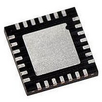
PIC18F27J13-I/ML Microchip Technology, PIC18F27J13-I/ML Datasheet - Page 291

PIC18F27J13-I/ML
Manufacturer Part Number
PIC18F27J13-I/ML
Description
IC PIC MCU 128KB FLASH 28QFN
Manufacturer
Microchip Technology
Series
PIC® XLP™ 18Fr
Datasheets
1.PIC18LF24J10-ISS.pdf
(32 pages)
2.PIC18F26J13-ISS.pdf
(496 pages)
3.PIC18F26J13-ISS.pdf
(558 pages)
4.PIC18F26J13-ISS.pdf
(12 pages)
Specifications of PIC18F27J13-I/ML
Core Size
8-Bit
Program Memory Size
128KB (64K x 16)
Core Processor
PIC
Speed
48MHz
Connectivity
I²C, LIN, SPI, UART/USART
Peripherals
Brown-out Detect/Reset, POR, PWM, WDT
Number Of I /o
22
Program Memory Type
FLASH
Ram Size
3.8K x 8
Voltage - Supply (vcc/vdd)
2.15 V ~ 3.6 V
Data Converters
A/D 10x10b/12b
Oscillator Type
Internal
Operating Temperature
-40°C ~ 85°C
Package / Case
*
Controller Family/series
PIC18
Cpu Speed
48MHz
Digital Ic Case Style
QFN
Supply Voltage Range
1.8V To 5.5V
Embedded Interface Type
I2C, SPI, USART
Rohs Compliant
Yes
Processor Series
PIC18F
Core
PIC
Data Bus Width
8 bit
Data Ram Size
4 KB
Interface Type
I2C, SPI, EUSART
Maximum Clock Frequency
48 MHz
Number Of Programmable I/os
19
Number Of Timers
8
Operating Supply Voltage
2 V to 3.6 V
Maximum Operating Temperature
+ 85 C
Mounting Style
SMD/SMT
3rd Party Development Tools
52715-96, 52716-328, 52717-734, 52712-325, EWPIC18
Development Tools By Supplier
DM164128, DM180021, DM183026-2, DV164131, MA180030, DM183022, DM183032, DV164136, MA180024
Minimum Operating Temperature
- 40 C
On-chip Adc
12 bit, 10 Channel
Lead Free Status / RoHS Status
Lead free / RoHS Compliant
For Use With
MA180030 - BOARD DEMO PIC18F47J13 FS USBMA180029 - BOARD DEMO PIC18F47J53 FS USB
Eeprom Size
-
Lead Free Status / Rohs Status
Details
Available stocks
Company
Part Number
Manufacturer
Quantity
Price
Company:
Part Number:
PIC18F27J13-I/ML
Manufacturer:
MICROCHIP
Quantity:
4 000
- PIC18LF24J10-ISS PDF datasheet
- PIC18F26J13-ISS PDF datasheet #2
- PIC18F26J13-ISS PDF datasheet #3
- PIC18F26J13-ISS PDF datasheet #4
- Current page: 291 of 496
- Download datasheet (5Mb)
17.0
The
conversion of an analog input signal to a 10-bit binary
representation of that signal. This device uses analog
inputs, which are multiplexed into a single sample and
hold circuit. The output of the sample and hold is
connected to the input of the converter. The converter
generates a 10-bit binary result via successive
approximation and stores the conversion result into the
ADC result registers (ADRESL and ADRESH).
FIGURE 17-1:
2010 Microchip Technology Inc.
Note: Additional ADC channels AN5-AN7 and AN20-AN27 are only available on PIC18(L)F4XK22 devices.
Analog-to-Digital
ANALOG-TO-DIGITAL
CONVERTER (ADC) MODULE
V
V
REF
REF
AN28
AN27
AN5
+/AN3
FVR BUF2
FVR BUF2
-/AN2
Reserved
AN4
Reserved
Reserved
AN3
AN2
AN1
AN0
Reserved
(1)
(1)
ADC BLOCK DIAGRAM
(1)
CTMU
A
A
VDD
VSS
Converter
11101
11100
11011
11111
11110
00101
00100
00011
00010
00001
00000
11
11
10
10
00
01
00
01
(ADC)
2
2
5
allows
Preliminary
PVCFG<1:0>
NVCFG<1:0>
CHS<4:0>
The ADC voltage reference is software selectable to
either V
pins.
The ADC can generate an interrupt upon completion of
a conversion. This interrupt can be used to wake-up the
device from Sleep.
Figure 17-1
10-Bit ADC
PIC18(L)F2X/4XK22
DD
or a voltage applied to the external reference
shows the block diagram of the ADC.
ADFM
10
ADCMD
GO/DONE
ADON
ADRESH
0 = Left Justify
1 = Right Justify
10
DS41412D-page 291
ADRESL
Related parts for PIC18F27J13-I/ML
Image
Part Number
Description
Manufacturer
Datasheet
Request
R

Part Number:
Description:
Manufacturer:
Microchip Technology Inc.
Datasheet:

Part Number:
Description:
Manufacturer:
Microchip Technology Inc.
Datasheet:

Part Number:
Description:
Manufacturer:
Microchip Technology Inc.
Datasheet:

Part Number:
Description:
Manufacturer:
Microchip Technology Inc.
Datasheet:

Part Number:
Description:
Manufacturer:
Microchip Technology Inc.
Datasheet:

Part Number:
Description:
Manufacturer:
Microchip Technology Inc.
Datasheet:

Part Number:
Description:
Manufacturer:
Microchip Technology Inc.
Datasheet:

Part Number:
Description:
Manufacturer:
Microchip Technology Inc.
Datasheet:


