PIC18F27J13-I/ML Microchip Technology, PIC18F27J13-I/ML Datasheet - Page 201
PIC18F27J13-I/ML
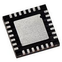
Manufacturer Part Number
PIC18F27J13-I/ML
Description
IC PIC MCU 128KB FLASH 28QFN
Manufacturer
Microchip Technology
Series
PIC® XLP™ 18Fr
Datasheets
1.PIC18LF24J10-ISS.pdf
(32 pages)
2.PIC18F26J13-ISS.pdf
(496 pages)
3.PIC18F26J13-ISS.pdf
(558 pages)
4.PIC18F26J13-ISS.pdf
(12 pages)
Specifications of PIC18F27J13-I/ML
Core Size
8-Bit
Program Memory Size
128KB (64K x 16)
Core Processor
PIC
Speed
48MHz
Connectivity
I²C, LIN, SPI, UART/USART
Peripherals
Brown-out Detect/Reset, POR, PWM, WDT
Number Of I /o
22
Program Memory Type
FLASH
Ram Size
3.8K x 8
Voltage - Supply (vcc/vdd)
2.15 V ~ 3.6 V
Data Converters
A/D 10x10b/12b
Oscillator Type
Internal
Operating Temperature
-40°C ~ 85°C
Package / Case
*
Controller Family/series
PIC18
Cpu Speed
48MHz
Digital Ic Case Style
QFN
Supply Voltage Range
1.8V To 5.5V
Embedded Interface Type
I2C, SPI, USART
Rohs Compliant
Yes
Processor Series
PIC18F
Core
PIC
Data Bus Width
8 bit
Data Ram Size
4 KB
Interface Type
I2C, SPI, EUSART
Maximum Clock Frequency
48 MHz
Number Of Programmable I/os
19
Number Of Timers
8
Operating Supply Voltage
2 V to 3.6 V
Maximum Operating Temperature
+ 85 C
Mounting Style
SMD/SMT
3rd Party Development Tools
52715-96, 52716-328, 52717-734, 52712-325, EWPIC18
Development Tools By Supplier
DM164128, DM180021, DM183026-2, DV164131, MA180030, DM183022, DM183032, DV164136, MA180024
Minimum Operating Temperature
- 40 C
On-chip Adc
12 bit, 10 Channel
Lead Free Status / RoHS Status
Lead free / RoHS Compliant
For Use With
MA180030 - BOARD DEMO PIC18F47J13 FS USBMA180029 - BOARD DEMO PIC18F47J53 FS USB
Eeprom Size
-
Lead Free Status / Rohs Status
Details
Available stocks
Company
Part Number
Manufacturer
Quantity
Price
Company:

Part Number:
PIC18F27J13-I/ML
Manufacturer:
MICROCHIP
Quantity:
4 000


TABLE 14-14: CONFIGURATION REGISTERS ASSOCIATED WITH CAPTURE
REGISTER 14-1:
2010 Microchip Technology Inc.
CONFIG3H
Legend: — = Unimplemented location, read as ‘0’. Shaded bits are not used by Capture mode.
bit 7
Legend:
R = Readable bit
u = Bit is unchanged
‘1’ = Bit is set
bit 7-6
bit 5-4
bit 3-0
Note 1:
Name
U-0
—
This feature is available on CCP5 only.
MCLRE
Bit 7
Unused
DCxB<1:0>: PWM Duty Cycle Least Significant bits
Capture mode:
Unused
Compare mode:
Unused
PWM mode:
These bits are the two LSbs of the PWM duty cycle. The eight MSbs are found in CCPRxL.
CCPxM<3:0>: ECCPx Mode Select bits
0000 = Capture/Compare/PWM off (resets the module)
0001 = Reserved
0010 = Compare mode: toggle output on match
0011 = Reserved
0100 = Capture mode: every falling edge
0101 = Capture mode: every rising edge
0110 = Capture mode: every 4th rising edge
0111 = Capture mode: every 16th rising edge
1000 = Compare mode: set output on compare match (CCPx pin is set, CCPxIF is set)
1001 = Compare mode: clear output on compare match (CCPx pin is cleared, CCPxIF is set)
1010 = Compare mode: generate software interrupt on compare match (CCPx pin is unaffected,
1011 = Compare mode: Special Event Trigger (CCPx pin is unaffected, CCPxIF is set)
11xx =: PWM mode
U-0
—
CCPxCON: STANDARD CCPx CONTROL REGISTER
CCPxIF is set)
Bit 6
—
W = Writable bit
x = Bit is unknown
‘0’ = Bit is cleared
R/W-0
P2BMX
Bit 5
DCxB<1:0>
TimerX (selected by CxTSEL bits) is reset
ADON is set, starting A/D conversion if A/D module is enabled
T3CMX
R/W-0
Bit 4
Preliminary
HFOFST
U = Unimplemented bit, read as ‘0’
-n/n = Value at POR and BOR/Value at all other Reset
Bit 3
R/W-0
PIC18(L)F2X/4XK22
CCP3MX
Bit 2
R/W-0
CCPxM<3:0>
PBADEN
Bit 1
R/W-0
CCP2MX
DS41412D-page 201
Bit 0
(1)
R/W-0
Register
on Page
354
bit 0
Related parts for PIC18F27J13-I/ML
Image
Part Number
Description
Manufacturer
Datasheet
Request
R

Part Number:
Description:
Manufacturer:
Microchip Technology Inc.
Datasheet:
Part Number:
Description:
Manufacturer:
Microchip Technology Inc.
Datasheet:
Part Number:
Description:
Manufacturer:
Microchip Technology Inc.
Datasheet:
Part Number:
Description:
Manufacturer:
Microchip Technology Inc.
Datasheet:
Part Number:
Description:
Manufacturer:
Microchip Technology Inc.
Datasheet:
Part Number:
Description:
Manufacturer:
Microchip Technology Inc.
Datasheet:
Part Number:
Description:
Manufacturer:
Microchip Technology Inc.
Datasheet:
Part Number:
Description:
Manufacturer:
Microchip Technology Inc.
Datasheet: