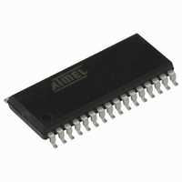
AT90PWM316-16SU Atmel, AT90PWM316-16SU Datasheet - Page 249

AT90PWM316-16SU
Manufacturer Part Number
AT90PWM316-16SU
Description
MCU AVR 16K ISP FLSH 16MHZ32SOIC
Manufacturer
Atmel
Series
AVR® 90PWM Lightingr
Datasheet
1.AT90PWM216-16SU.pdf
(359 pages)
Specifications of AT90PWM316-16SU
Core Processor
AVR
Core Size
8-Bit
Speed
16MHz
Connectivity
SPI, UART/USART
Peripherals
Brown-out Detect/Reset, POR, PWM, WDT
Number Of I /o
27
Program Memory Size
16KB (16K x 8)
Program Memory Type
FLASH
Eeprom Size
512 x 8
Ram Size
1K x 8
Voltage - Supply (vcc/vdd)
2.7 V ~ 5.5 V
Data Converters
A/D 11x10b; D/A 1x10b
Oscillator Type
Internal
Operating Temperature
-40°C ~ 105°C
Package / Case
32-SOIC (7.5mm Width)
Processor Series
AT90PWMx
Core
AVR8
Data Bus Width
8 bit
Data Ram Size
1 KB
Interface Type
SPI, UART
Maximum Clock Frequency
16 MHz
Number Of Programmable I/os
53
Number Of Timers
2
Operating Supply Voltage
2.7 V to 5.5 V
Maximum Operating Temperature
+ 105 C
Mounting Style
SMD/SMT
3rd Party Development Tools
EWAVR, EWAVR-BL
Development Tools By Supplier
ATAVRDRAGON, ATSTK500, ATSTK600, ATAVRISP2, ATAVRONEKIT, ATAVRFBKIT, ATAVRISP2
Minimum Operating Temperature
- 40 C
On-chip Adc
10 bit, 11 Channel
Package
32SOIC
Device Core
AVR
Family Name
90P
Maximum Speed
16 MHz
For Use With
ATSTK600-SOIC - STK600 SOCKET/ADAPTER FOR SOIC770-1007 - ISP 4PORT ATMEL AVR MCU SPI/JTAG770-1005 - ISP 4PORT FOR ATMEL AVR MCU JTAG770-1004 - ISP 4PORT FOR ATMEL AVR MCU SPIATAVRMC200 - KIT EVAL FOR AT90PWM3 ASYNCATAVRFBKIT - KIT DEMO BALLAST FOR AT90PWM2ATAVRISP2 - PROGRAMMER AVR IN SYSTEM
Lead Free Status / RoHS Status
Lead free / RoHS Compliant
Available stocks
Company
Part Number
Manufacturer
Quantity
Price
Part Number:
AT90PWM316-16SU
Manufacturer:
ATMEL/爱特梅尔
Quantity:
20 000
- Current page: 249 of 359
- Download datasheet (6Mb)
7710E–AVR–08/10
These 2 bits determine the voltage reference for the ADC.
The different setting are shown in
Table 21-3.
If these bits are changed during a conversion, the change will not take effect until this conversion
is complete (it means while the ADIF bit in ADCSRA register is set).
In case the internal Vref is selected, it is turned ON as soon as an analog feature needed it is
set.
• Bit 5 – ADLAR: ADC Left Adjust Result
Set this bit to left adjust the ADC result.
Clear it to right adjust the ADC result.
The ADLAR bit affects the configuration of the ADC result data registers. Changing this bit
affects the ADC data registers immediately regardless of any on going conversion. For a com-
plete description of this bit, see Section “ADC Result Data Registers – ADCH and ADCL”,
page 252.
• Bit 3, 2, 1, 0 – MUX3, MUX2, MUX1, MUX0: ADC Channel Selection Bits
These 4 bits determine which analog inputs are connected to the ADC input. The different set-
ting are shown in
Table 21-4.
REFS1
0
0
1
1
MUX3
0
0
0
0
0
0
0
0
1
1
1
1
1
ADC Voltage Reference Selection
ADC Input Channel Selection
REFS0
0
1
0
1
MUX2
0
0
0
0
1
1
1
1
0
0
0
0
1
Table
21-4.
Description
External Vref on AREF pin, Internal Vref is switched off
AVcc with external capacitor connected on the AREF pin
Reserved
Internal 2.56V Reference voltage with external capacitor connected on
the AREF pin
MUX1
0
0
1
1
0
0
1
1
0
0
1
1
0
Table
21-3.
MUX0
0
1
0
1
0
1
0
1
0
1
0
1
0
Description
ADC0
ADC1
ADC2
ADC3
ADC4
ADC5
ADC6
ADC7
ADC8
ADC9
ADC10
AMP0
AMP1 (- is ADC8, + is ADC9)
AT90PWM216/316
249
Related parts for AT90PWM316-16SU
Image
Part Number
Description
Manufacturer
Datasheet
Request
R

Part Number:
Description:
IC AVR MCU FLASH 8K 32QFN
Manufacturer:
Atmel
Datasheet:

Part Number:
Description:
IC AVR MCU FLASH 8K 32SOIC
Manufacturer:
Atmel
Datasheet:

Part Number:
Description:
MCU AVR 8K FLASH 16MHZ 32-QFN
Manufacturer:
Atmel
Datasheet:

Part Number:
Description:
DEV KIT FOR AVR/AVR32
Manufacturer:
Atmel
Datasheet:

Part Number:
Description:
INTERVAL AND WIPE/WASH WIPER CONTROL IC WITH DELAY
Manufacturer:
ATMEL Corporation
Datasheet:

Part Number:
Description:
Low-Voltage Voice-Switched IC for Hands-Free Operation
Manufacturer:
ATMEL Corporation
Datasheet:

Part Number:
Description:
MONOLITHIC INTEGRATED FEATUREPHONE CIRCUIT
Manufacturer:
ATMEL Corporation
Datasheet:

Part Number:
Description:
AM-FM Receiver IC U4255BM-M
Manufacturer:
ATMEL Corporation
Datasheet:

Part Number:
Description:
Monolithic Integrated Feature Phone Circuit
Manufacturer:
ATMEL Corporation
Datasheet:

Part Number:
Description:
Multistandard Video-IF and Quasi Parallel Sound Processing
Manufacturer:
ATMEL Corporation
Datasheet:

Part Number:
Description:
High-performance EE PLD
Manufacturer:
ATMEL Corporation
Datasheet:

Part Number:
Description:
8-bit Flash Microcontroller
Manufacturer:
ATMEL Corporation
Datasheet:


