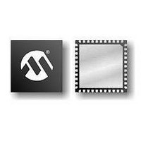
PIC18F47J53T-I/ML Microchip Technology, PIC18F47J53T-I/ML Datasheet - Page 461

PIC18F47J53T-I/ML
Manufacturer Part Number
PIC18F47J53T-I/ML
Description
IC MCU 8BIT 128KB FLASH 44 QFN
Manufacturer
Microchip Technology
Series
PIC® XLP™ 18Fr
Specifications of PIC18F47J53T-I/ML
Program Memory Type
FLASH
Program Memory Size
128KB (64K x 16)
Package / Case
*
Core Processor
PIC
Core Size
8-Bit
Speed
48MHz
Connectivity
I²C, LIN, SPI, UART/USART, USB
Peripherals
Brown-out Detect/Reset, POR, PWM, WDT
Number Of I /o
34
Ram Size
3.8K x 8
Voltage - Supply (vcc/vdd)
2.15 V ~ 3.6 V
Data Converters
A/D 13x10b/12b
Oscillator Type
Internal
Operating Temperature
-40°C ~ 85°C
Processor Series
PIC18F
Core
PIC
Data Bus Width
8 bit
Data Ram Size
3.8 KB
Interface Type
I2C, SPI, USART
Maximum Clock Frequency
48 MHz
Number Of Programmable I/os
22
Number Of Timers
8
Operating Supply Voltage
2.15 V to 3.6 V
Maximum Operating Temperature
+ 85 C
Mounting Style
SMD/SMT
3rd Party Development Tools
52715-96, 52716-328, 52717-734, 52712-325, EWPIC18
Minimum Operating Temperature
- 40 C
Lead Free Status / RoHS Status
Lead free / RoHS Compliant
For Use With
MA180029 - BOARD DEMO PIC18F47J53 FS USB
Eeprom Size
-
Lead Free Status / Rohs Status
Lead free / RoHS Compliant
Available stocks
Company
Part Number
Manufacturer
Quantity
Price
Company:
Part Number:
PIC18F47J53T-I/ML
Manufacturer:
MURATA
Quantity:
640 000
- Current page: 461 of 586
- Download datasheet (6Mb)
TABLE 29-1:
FIGURE 29-1:
2010 Microchip Technology Inc.
[expr]<n>
< >
italics
Field
Byte-oriented file register operations
Byte to Byte move operations (2-word)
OPCODE FIELD DESCRIPTIONS (CONTINUED)
Bit-oriented file register operations
Literal operations
CALL, GOTO and Branch operations
Control operations
15
15
15
15
15
15
15
15
15
15
OPCODE b (BIT #) a
Specifies bit n of the register indicated by the pointer expr.
Assigned to.
Register bit field.
In the set of.
User-defined term (font is Courier New).
OPCODE
GENERAL FORMAT FOR INSTRUCTIONS
k = 8-bit immediate value
n = 20-bit immediate value
1111
OPCODE
b = 3-bit position of bit in file register (f)
a = 0 to force Access Bank
a = 1 for BSR to select bank
f = 8-bit file register address
d = 0 for result destination to be WREG register
d = 1 for result destination to be file register (f)
a = 0 to force Access Bank
a = 1 for BSR to select bank
f = 12-bit file register address
f = 8-bit file register address
1111
1111
OPCODE
OPCODE
12 11
OPCODE
12 11
12 11
S = Fast bit
12 11
10
12 11
11 10
d
9
9 8 7
f (Destination FILE #)
8
f (Source FILE #)
a
8 7
8 7
7
8 7
S
n<19:8> (literal)
n<19:8> (literal)
n<7:0> (literal)
k (literal)
n<7:0> (literal)
f (FILE #)
f (FILE #)
Preliminary
0
0
PIC18F47J53 FAMILY
0
0
0
0
0
0
0
0
Description
ADDWF MYREG, W, B
MOVFF MYREG1, MYREG2
BSF MYREG, bit, B
MOVLW 7Fh
GOTO Label
CALL MYFUNC
Example Instruction
DS39964B-page 461
Related parts for PIC18F47J53T-I/ML
Image
Part Number
Description
Manufacturer
Datasheet
Request
R

Part Number:
Description:
Manufacturer:
Microchip Technology Inc.
Datasheet:

Part Number:
Description:
Manufacturer:
Microchip Technology Inc.
Datasheet:

Part Number:
Description:
Manufacturer:
Microchip Technology Inc.
Datasheet:

Part Number:
Description:
Manufacturer:
Microchip Technology Inc.
Datasheet:

Part Number:
Description:
Manufacturer:
Microchip Technology Inc.
Datasheet:

Part Number:
Description:
Manufacturer:
Microchip Technology Inc.
Datasheet:

Part Number:
Description:
Manufacturer:
Microchip Technology Inc.
Datasheet:

Part Number:
Description:
Manufacturer:
Microchip Technology Inc.
Datasheet:


