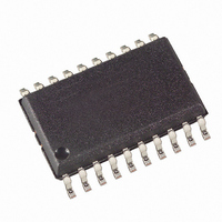
ATTINY861V-10SU Atmel, ATTINY861V-10SU Datasheet - Page 66

ATTINY861V-10SU
Manufacturer Part Number
ATTINY861V-10SU
Description
IC MCU AVR 8K FLASH 10MHZ 20SOIC
Manufacturer
Atmel
Series
AVR® ATtinyr
Specifications of ATTINY861V-10SU
Core Processor
AVR
Core Size
8-Bit
Speed
10MHz
Connectivity
USI
Peripherals
Brown-out Detect/Reset, POR, PWM, WDT
Number Of I /o
16
Program Memory Size
8KB (4K x 16)
Program Memory Type
FLASH
Eeprom Size
512 x 8
Ram Size
512 x 8
Voltage - Supply (vcc/vdd)
1.8 V ~ 5.5 V
Data Converters
A/D 11x10b
Oscillator Type
Internal
Operating Temperature
-40°C ~ 85°C
Package / Case
20-SOIC (7.5mm Width)
Processor Series
ATTINY8x
Core
AVR8
Data Bus Width
8 bit
Data Ram Size
512 B
Interface Type
2-Wire, SPI, USI
Maximum Clock Frequency
10 MHz
Number Of Programmable I/os
16
Number Of Timers
2
Maximum Operating Temperature
+ 85 C
Mounting Style
SMD/SMT
Minimum Operating Temperature
- 40 C
On-chip Adc
10 bit, 11 Channel
Package
20SOIC
Device Core
AVR
Family Name
ATtiny
Maximum Speed
10 MHz
Operating Supply Voltage
2.5|3.3|5 V
For Use With
ATSTK600-DIP40 - STK600 SOCKET/ADAPTER 40-PDIPATAVRBC100 - REF DESIGN KIT BATTERY CHARGER770-1007 - ISP 4PORT ATMEL AVR MCU SPI/JTAG770-1004 - ISP 4PORT FOR ATMEL AVR MCU SPI
Lead Free Status / RoHS Status
Lead free / RoHS Compliant
Available stocks
Company
Part Number
Manufacturer
Quantity
Price
Company:
Part Number:
ATTINY861V-10SU
Manufacturer:
Atmel
Quantity:
2 881
Company:
Part Number:
ATTINY861V-10SUR
Manufacturer:
Atmel
Quantity:
1 499
- Current page: 66 of 242
- Download datasheet (5Mb)
10.2.2
66
ATtiny261/461/861
Alternate Functions of Port B
The Port B pins with alternate function are shown in
Table 10-6.
• Port B, Bit 7 – RESET/ dW/ ADC10/ PCINT15
• RESET, Reset pin: When the RSTDISBL Fuse is programmed, this pin functions as a normal
• If PB7 is used as a reset pin, DDB7, PORTB7 and PINB7 will all read 0.
• dW: When the debugWIRE Enable (DWEN) Fuse is programmed and Lock bits are
I/O pin, and the part will have to rely on Power-on Reset and Brown-out Reset as its reset
sources. When the RSTDISBL Fuse is unprogrammed, the reset circuitry is connected to the
pin, and the pin can not be used as an I/O pin.
unprogrammed, the RESET port pin is configured as a wire-AND (open-drain) bi-directional
I/O pin with pull-up enabled and becomes the communication gateway between target and
emulator.
Port Pin
PB7
PB6
PB5
PB4
PB3
PB2
PB1
PB0
Port B Pins Alternate Functions
Alternate Function
RESET: Reset pin
dW:
ADC10: ADC Input Channel 10
PCINT15:Pin Change Interrupt 0, Source 15
ADC9:
T0:
INT0:
PCINT14:Pin Change Interrupt 0, Source 14
XTAL2: Crystal Oscillator Output
CLKO: System Clock Output
OC1D: Timer/Counter1 Compare Match D Output
ADC8:
PCINT13:Pin Change Interrupt 0, Source 13
XTAL1: Crystal Oscillator Input
CLKI:
OC1D: Inverted Timer/Counter1 Compare Match D Output
ADC7:
PCINT12:Pin Change Interrupt 0, Source 12
OC1B: Timer/Counter1 Compare Match B Output
PCINT11:Pin Change Interrupt 0, Source 11
USCK: USI Clock (Three Wire Mode)
SCL :
OC1B: Inverted Timer/Counter1 Compare Match B Output
PCINT10:Pin Change Interrupt 0, Source 10
DO:
OC1A: Timer/Counter1 Compare Match A Output
PCINT9: Pin Change Interrupt 1, Source 9
DI:
SDA:
OC1A: Inverted Timer/Counter1 Compare Match A Output
PCINT8: Pin Change Interrupt 1, Source 8
debugWire I/O
ADC Input Channel 9
Timer/Counter0 Clock Source
External Interrupt 0 Input
ADC Input Channel 8
External Clock Input
ADC Input Channel 7
USI Clock (Two Wire Mode)
USI Data Output (Three Wire Mode)
USI Data Input (Three Wire Mode)
USI Data Input (Two Wire Mode)
Table
10-6.
2588E–AVR–08/10
Related parts for ATTINY861V-10SU
Image
Part Number
Description
Manufacturer
Datasheet
Request
R

Part Number:
Description:
Manufacturer:
Atmel Corporation
Datasheet:

Part Number:
Description:
Manufacturer:
Atmel Corporation
Datasheet:

Part Number:
Description:
IC MCU AVR 8K FLASH 20MHZ 32-QFN
Manufacturer:
Atmel
Datasheet:

Part Number:
Description:
IC MCU AVR 8K FLASH 20MHZ 20SOIC
Manufacturer:
Atmel
Datasheet:

Part Number:
Description:
MCU AVR 8K FLASH 15MHZ 32-QFN
Manufacturer:
Atmel
Datasheet:

Part Number:
Description:
MCU AVR 8K FLASH 15MHZ 20-SOIC
Manufacturer:
Atmel
Datasheet:

Part Number:
Description:
MCU AVR 8KB FLASH 15MHZ 32-VQFN
Manufacturer:
Atmel
Datasheet:

Part Number:
Description:
Microcontrollers (MCU) 8kB Flash 0.512kB EEPROM 16 I/O Pins
Manufacturer:
Atmel
Datasheet:

Part Number:
Description:
8-bit Microcontrollers - MCU 8KB FL 512B EE 512B SRAM 20MHZ IND 5V
Manufacturer:
Atmel

Part Number:
Description:
IC, MCU, 8BIT, 2K FLASH, 20SOIC
Manufacturer:
Atmel
Datasheet:


