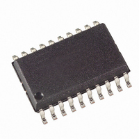
ATTINY861V-10SU Atmel, ATTINY861V-10SU Datasheet - Page 136

ATTINY861V-10SU
Manufacturer Part Number
ATTINY861V-10SU
Description
IC MCU AVR 8K FLASH 10MHZ 20SOIC
Manufacturer
Atmel
Series
AVR® ATtinyr
Specifications of ATTINY861V-10SU
Core Processor
AVR
Core Size
8-Bit
Speed
10MHz
Connectivity
USI
Peripherals
Brown-out Detect/Reset, POR, PWM, WDT
Number Of I /o
16
Program Memory Size
8KB (4K x 16)
Program Memory Type
FLASH
Eeprom Size
512 x 8
Ram Size
512 x 8
Voltage - Supply (vcc/vdd)
1.8 V ~ 5.5 V
Data Converters
A/D 11x10b
Oscillator Type
Internal
Operating Temperature
-40°C ~ 85°C
Package / Case
20-SOIC (7.5mm Width)
Processor Series
ATTINY8x
Core
AVR8
Data Bus Width
8 bit
Data Ram Size
512 B
Interface Type
2-Wire, SPI, USI
Maximum Clock Frequency
10 MHz
Number Of Programmable I/os
16
Number Of Timers
2
Maximum Operating Temperature
+ 85 C
Mounting Style
SMD/SMT
Minimum Operating Temperature
- 40 C
On-chip Adc
10 bit, 11 Channel
Package
20SOIC
Device Core
AVR
Family Name
ATtiny
Maximum Speed
10 MHz
Operating Supply Voltage
2.5|3.3|5 V
For Use With
ATSTK600-DIP40 - STK600 SOCKET/ADAPTER 40-PDIPATAVRBC100 - REF DESIGN KIT BATTERY CHARGER770-1007 - ISP 4PORT ATMEL AVR MCU SPI/JTAG770-1004 - ISP 4PORT FOR ATMEL AVR MCU SPI
Lead Free Status / RoHS Status
Lead free / RoHS Compliant
Available stocks
Company
Part Number
Manufacturer
Quantity
Price
Company:
Part Number:
ATTINY861V-10SU
Manufacturer:
Atmel
Quantity:
2 881
Company:
Part Number:
ATTINY861V-10SUR
Manufacturer:
Atmel
Quantity:
1 499
- Current page: 136 of 242
- Download datasheet (5Mb)
13.5.5
136
ATtiny261/461/861
USIPP – USI Pin Position
Table 13-2.
• Bit 1 – USICLK: Clock Strobe
Writing a one to this bit location strobes the USI Data Register to shift one step and the counter
to increment by one, provided that the USICS1:0 bits are set to zero and by doing so the soft-
ware clock strobe option is selected. The output will change immediately when the clock strobe
is executed, i.e., in the same instruction cycle. The value shifted into the USI Data Register is
sampled the previous instruction cycle. The bit will be read as zero.
When an external clock source is selected (USICS1 = 1), the USICLK function is changed from
a clock strobe to a Clock Select Register. Setting the USICLK bit in this case will select the
USITC strobe bit as clock source for the 4-bit counter (see
• Bit 0 – USITC: Toggle Clock Port Pin
Writing a one to this bit location toggles the USCK/SCL value either from 0 to 1, or from 1 to 0.
The toggling is independent of the setting in the Data Direction Register, but if the PORT value is
to be shown on the pin the DDB2 must be set as output (to one). This feature allows easy clock
generation when implementing master devices. The bit will be read as zero.
When an external clock source is selected (USICS1 = 1) and the USICLK bit is set to one, writ-
ing to the USITC strobe bit will directly clock the 4-bit counter. This allows an early detection of
when the transfer is done when operating as a master device.
• Bits 7:1 – Res: Reserved Bits
These bits are reserved and will always read as zero.
• Bit 0 – USIPOS: USI Pin Position
Setting this bit to one changes the USI pin position. As default pins PB2:PB0 are used for the
USI pin functions, but when writing this bit to one the USIPOS bit is set the USI pin functions are
on pins PA2:PA0.
Bit
0x11 (0x31)
Read/Write
Initial Value
USICS1
1
1
1
USICS0
Relations between the USICS1:0 and USICLK Setting (Continued)
1
0
1
R
7
0
-
USICLK
R
6
0
-
0
1
1
USI Data Register Clock
Source
External, negative edge
External, positive edge
External, negative edge
R
5
0
-
R
4
0
-
R
3
0
-
Table
R
2
0
-
13-2).
4-bit Counter Clock Source
External, both edges
Software clock strobe (USITC)
Software clock strobe (USITC)
R
1
0
-
USIPOS
R/W
0
0
2588E–AVR–08/10
USIPP
Related parts for ATTINY861V-10SU
Image
Part Number
Description
Manufacturer
Datasheet
Request
R

Part Number:
Description:
Manufacturer:
Atmel Corporation
Datasheet:

Part Number:
Description:
Manufacturer:
Atmel Corporation
Datasheet:

Part Number:
Description:
IC MCU AVR 8K FLASH 20MHZ 32-QFN
Manufacturer:
Atmel
Datasheet:

Part Number:
Description:
IC MCU AVR 8K FLASH 20MHZ 20SOIC
Manufacturer:
Atmel
Datasheet:

Part Number:
Description:
MCU AVR 8K FLASH 15MHZ 32-QFN
Manufacturer:
Atmel
Datasheet:

Part Number:
Description:
MCU AVR 8K FLASH 15MHZ 20-SOIC
Manufacturer:
Atmel
Datasheet:

Part Number:
Description:
MCU AVR 8KB FLASH 15MHZ 32-VQFN
Manufacturer:
Atmel
Datasheet:

Part Number:
Description:
Microcontrollers (MCU) 8kB Flash 0.512kB EEPROM 16 I/O Pins
Manufacturer:
Atmel
Datasheet:

Part Number:
Description:
8-bit Microcontrollers - MCU 8KB FL 512B EE 512B SRAM 20MHZ IND 5V
Manufacturer:
Atmel

Part Number:
Description:
IC, MCU, 8BIT, 2K FLASH, 20SOIC
Manufacturer:
Atmel
Datasheet:


