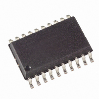
ATTINY461V-10SU Atmel, ATTINY461V-10SU Datasheet - Page 53

ATTINY461V-10SU
Manufacturer Part Number
ATTINY461V-10SU
Description
IC MCU AVR 4K FLASH 10MHZ 20SOIC
Manufacturer
Atmel
Series
AVR® ATtinyr
Specifications of ATTINY461V-10SU
Core Processor
AVR
Core Size
8-Bit
Speed
10MHz
Connectivity
USI
Peripherals
Brown-out Detect/Reset, POR, PWM, WDT
Number Of I /o
16
Program Memory Size
4KB (2K x 16)
Program Memory Type
FLASH
Eeprom Size
256 x 8
Ram Size
256 x 8
Voltage - Supply (vcc/vdd)
1.8 V ~ 5.5 V
Data Converters
A/D 11x10b
Oscillator Type
Internal
Operating Temperature
-40°C ~ 85°C
Package / Case
20-SOIC (7.5mm Width)
Processor Series
ATTINY4x
Core
AVR8
Data Bus Width
8 bit
Data Ram Size
256 B
Interface Type
2-Wire, SPI, USI
Maximum Clock Frequency
10 MHz
Number Of Programmable I/os
16
Number Of Timers
2
Operating Supply Voltage
2.7 V to 5.5 V
Maximum Operating Temperature
+ 85 C
Mounting Style
SMD/SMT
Minimum Operating Temperature
- 40 C
On-chip Adc
10 bit
Package
20SOIC W
Device Core
AVR
Family Name
ATtiny
Maximum Speed
10 MHz
For Use With
ATSTK600 - DEV KIT FOR AVR/AVR32ATAVRBC100 - REF DESIGN KIT BATTERY CHARGER770-1007 - ISP 4PORT ATMEL AVR MCU SPI/JTAG770-1004 - ISP 4PORT FOR ATMEL AVR MCU SPI
Lead Free Status / RoHS Status
Lead free / RoHS Compliant
Available stocks
Company
Part Number
Manufacturer
Quantity
Price
Part Number:
ATTINY461V-10SU
Manufacturer:
ATMEL/爱特梅尔
Quantity:
20 000
Part Number:
ATTINY461V-10SUR
Manufacturer:
ATMEL/爱特梅尔
Quantity:
20 000
9.3.3
2588E–AVR–08/10
GIFR – General Interrupt Flag Register
Control Register (MCUCR) define whether the external interrupt is activated on rising and/or fall-
ing edge of the INT0 pin or level sensed. Activity on the pin will cause an interrupt request even
if INT0 is configured as an output. The corresponding interrupt of External Interrupt Request 0 is
executed from the INT0 Interrupt Vector.
• Bit 5 – PCIE1: Pin Change Interrupt Enable
When the PCIE1 bit is set (one) and the I-bit in the Status Register (SREG) is set (one), pin
change interrupt is enabled. Any change on any enabled PCINT7:0 or PCINT15:12 pin will
cause an interrupt. The corresponding interrupt of Pin Change Interrupt Request is executed
from the PCI Interrupt Vector. PCINT7:0 and PCINT15:12 pins are enabled individually by the
PCMSK0 and PCMSK1 Register.
• Bit 4 – PCIE0: Pin Change Interrupt Enable
When the PCIE0 bit is set (one) and the I-bit in the Status Register (SREG) is set (one), pin
change interrupt is enabled. Any change on any enabled PCINT11:8 pin will cause an interrupt.
The corresponding interrupt of Pin Change Interrupt Request is executed from the PCI Interrupt
Vector. PCINT11:8 pins are enabled individually by the PCMSK1 Register.
• Bits 3:0 – Res: Reserved Bits
These bits are reserved and will always read as zero.
• Bit 7 – INTF1: External Interrupt Flag 1
When an edge or logic change on the INT1 pin triggers an interrupt request, INTF1 becomes set
(one). If the I-bit in SREG and the INT1 bit in GIMSK are set (one), the MCU will jump to the cor-
responding Interrupt Vector. The flag is cleared when the interrupt routine is executed.
Alternatively, the flag can be cleared by writing a logical one to it. This flag is always cleared
when INT1 is configured as a level interrupt.
• Bit 6 – INTF0: External Interrupt Flag 0
When an edge or logic change on the INT0 pin triggers an interrupt request, INTF0 becomes set
(one). If the I-bit in SREG and the INT0 bit in GIMSK are set (one), the MCU will jump to the cor-
responding Interrupt Vector. The flag is cleared when the interrupt routine is executed.
Alternatively, the flag can be cleared by writing a logical one to it. This flag is always cleared
when INT0 is configured as a level interrupt.
• Bit 5 – PCIF: Pin Change Interrupt Flag
When a logic change on any PCINT15 pin triggers an interrupt request, PCIF becomes set
(one). If the I-bit in SREG and the PCIE bit in GIMSK are set (one), the MCU will jump to the cor-
responding Interrupt Vector. The flag is cleared when the interrupt routine is executed.
Alternatively, the flag can be cleared by writing a logical one to it.
• Bits 4:0 – Res: Reserved Bits
These bits are reserved and will always read as zero.
Bit
0x3A (0x5A)
Read/Write
Initial Value
7
INT1
R/W
0
6
INTF0
R/W
0
5
PCIF
R/W
0
4
–
R
0
3
–
R
0
2
–
R
0
1
–
R
0
0
–
R
0
GIFR
53


