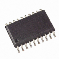
ATTINY461-20SU Atmel, ATTINY461-20SU Datasheet - Page 103

ATTINY461-20SU
Manufacturer Part Number
ATTINY461-20SU
Description
IC MCU AVR 4K FLASH 20MHZ 20SOIC
Manufacturer
Atmel
Series
AVR® ATtinyr
Datasheet
1.ATAVRMC321.pdf
(242 pages)
Specifications of ATTINY461-20SU
Core Processor
AVR
Core Size
8-Bit
Speed
20MHz
Connectivity
USI
Peripherals
Brown-out Detect/Reset, POR, PWM, WDT
Number Of I /o
16
Program Memory Size
4KB (2K x 16)
Program Memory Type
FLASH
Eeprom Size
256 x 8
Ram Size
256 x 8
Voltage - Supply (vcc/vdd)
2.7 V ~ 5.5 V
Data Converters
A/D 11x10b
Oscillator Type
Internal
Operating Temperature
-40°C ~ 85°C
Package / Case
20-SOIC (7.5mm Width)
Processor Series
ATTINY4x
Core
AVR8
Data Bus Width
8 bit
Data Ram Size
256 B
Interface Type
2-Wire, SPI, USI
Maximum Clock Frequency
20 MHz
Number Of Programmable I/os
16
Number Of Timers
2
Operating Supply Voltage
2.7 V to 5.5 V
Maximum Operating Temperature
+ 85 C
Mounting Style
SMD/SMT
3rd Party Development Tools
EWAVR, EWAVR-BL
Development Tools By Supplier
ATAVRDRAGON, ATSTK500, ATSTK600, ATAVRISP2, ATAVRONEKIT
Minimum Operating Temperature
- 40 C
On-chip Adc
10 bit, 16 Channel
Package
20SOIC
Device Core
AVR
Family Name
ATtiny
Maximum Speed
20 MHz
For Use With
ATSTK600-DIP40 - STK600 SOCKET/ADAPTER 40-PDIPATAVRBC100 - REF DESIGN KIT BATTERY CHARGER770-1007 - ISP 4PORT ATMEL AVR MCU SPI/JTAG770-1004 - ISP 4PORT FOR ATMEL AVR MCU SPI
Lead Free Status / RoHS Status
Lead free / RoHS Compliant
Available stocks
Company
Part Number
Manufacturer
Quantity
Price
Company:
Part Number:
ATTINY461-20SU
Manufacturer:
ATMEL
Quantity:
3 282
- Current page: 103 of 242
- Download datasheet (5Mb)
2588E–AVR–08/10
Figure 12-13. Phase and Frequency Correct PWM Mode, Timing Diagram
The Timer/Counter Overflow Flag (TOV1) is set each time the counter reaches BOTTOM. The
Interrupt Flag can be used to generate an interrupt each time the counter reaches the BOTTOM
value.
In the Phase and Frequency Correct PWM mode, the compare unit allows generation of PWM
waveforms on the OC1x pins. Setting the COM1x1:0 bits to two will produce a non-inverted
PWM and setting the COM1x1:0 to three will produce an inverted PWM output. Setting the
COM1A1:0 bits to one will enable complementary Compare Output mode and produce both the
non-inverted (OC1x) and inverted output (OC1x). The actual values will only be visible on the
port pin if the data direction for the port pin is set as output. The PWM waveform is generated by
clearing (or setting) the Waveform Output (OCW1x) at the Compare Match between OCR1x and
TCNT1 when the counter increments, and setting (or clearing) the Waveform Output at Compare
Match when the counter decrements. The PWM frequency for the output when using the Phase
and Frequency Correct PWM can be calculated by the following equation:
The N variable represents the number of steps in dual-slope operation. The value of N equals to
the TOP value.
The extreme values for the OCR1C Register represent special cases when generating a PWM
waveform output in the Phase and Frequency Correct PWM mode. If the OCR1C is set equal to
BOTTOM, the output will be continuously low and if set equal to MAX the output will be continu-
ously high for non-inverted PWM mode. For inverted PWM the output will have the opposite
logic values.
The general I/O port function is overridden by the Output Compare value (OC1x / OC1x) from
the Dead Time Generator, if either of the COM1x1:0 bits are set and the Data Direction Register
bits for the OC1X and OC1X pins are set as an output. If the COM1x1:0 bits are cleared, the
TCNTn
OCWnx
(COMnx = 2)
OCWnx
Period
(COMnx = 3)
1
f
OCnxPCPWM
2
=
f
------------ -
clkT1
N
3
OCnx Interrupt Flag Set
OCRnx Update
TOVn Interrupt Flag Set
103
Related parts for ATTINY461-20SU
Image
Part Number
Description
Manufacturer
Datasheet
Request
R

Part Number:
Description:
Manufacturer:
Atmel Corporation
Datasheet:

Part Number:
Description:
Manufacturer:
Atmel Corporation
Datasheet:

Part Number:
Description:
IC AVR MCU 4K 20MHZ 32-QFN
Manufacturer:
Atmel
Datasheet:

Part Number:
Description:
MCU AVR 4K FLASH 15MHZ 32-QFN
Manufacturer:
Atmel
Datasheet:

Part Number:
Description:
MCU AVR 4KB FLASH 15MHZ 32-VQFN
Manufacturer:
Atmel
Datasheet:

Part Number:
Description:
MCU AVR 4KB FLASH 20MHZ 20SOIC
Manufacturer:
Atmel
Datasheet:

Part Number:
Description:
IC MCU AVR 4K 20MHZ 32QFN
Manufacturer:
Atmel
Datasheet:

Part Number:
Description:
Microcontrollers (MCU) 4kB Flash 0.256kB EEPROM 16 I/O Pins
Manufacturer:
Atmel
Datasheet:

Part Number:
Description:
IC, MCU, 8BIT, 2K FLASH, 20SOIC
Manufacturer:
Atmel
Datasheet:

Part Number:
Description:
IC, MCU, 8BIT, 2K FLASH, 20PDIP
Manufacturer:
Atmel
Datasheet:


