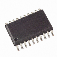
ATTINY261V-10SU Atmel, ATTINY261V-10SU Datasheet - Page 146

ATTINY261V-10SU
Manufacturer Part Number
ATTINY261V-10SU
Description
IC MCU AVR 2K FLASH 10MHZ 20SOIC
Manufacturer
Atmel
Series
AVR® ATtinyr
Datasheet
1.ATAVRMC321.pdf
(242 pages)
Specifications of ATTINY261V-10SU
Core Processor
AVR
Core Size
8-Bit
Speed
10MHz
Connectivity
USI
Peripherals
Brown-out Detect/Reset, POR, PWM, WDT
Number Of I /o
16
Program Memory Size
2KB (1K x 16)
Program Memory Type
FLASH
Eeprom Size
128 x 8
Ram Size
128 x 8
Voltage - Supply (vcc/vdd)
1.8 V ~ 5.5 V
Data Converters
A/D 11x10b
Oscillator Type
Internal
Operating Temperature
-40°C ~ 85°C
Package / Case
20-SOIC (7.5mm Width)
Package
20SOIC
Device Core
AVR
Family Name
ATtiny
Maximum Speed
10 MHz
Operating Supply Voltage
2.5|3.3|5 V
Data Bus Width
8 Bit
Number Of Programmable I/os
16
Interface Type
USI
On-chip Adc
11-chx10-bit
Number Of Timers
2
For Use With
ATSTK600 - DEV KIT FOR AVR/AVR32ATAVRBC100 - REF DESIGN KIT BATTERY CHARGER770-1007 - ISP 4PORT ATMEL AVR MCU SPI/JTAG770-1004 - ISP 4PORT FOR ATMEL AVR MCU SPIATSTK505 - ADAPTER KIT FOR 14PIN AVR MCU
Lead Free Status / RoHS Status
Lead free / RoHS Compliant
Available stocks
Company
Part Number
Manufacturer
Quantity
Price
Company:
Part Number:
ATTINY261V-10SU
Manufacturer:
Atmel
Quantity:
3 989
Part Number:
ATTINY261V-10SU
Manufacturer:
ATMEL/爱特梅尔
Quantity:
20 000
- Current page: 146 of 242
- Download datasheet (5Mb)
146
ATtiny261/461/861
Figure 15-3. ADC Prescaler
When initiating a single ended conversion by setting the ADSC bit in ADCSRA, the conversion
starts at the following rising edge of the ADC clock cycle.
A normal conversion takes 13 ADC clock cycles. The first conversion after the ADC is switched
on (ADEN in ADCSRA is set) takes 25 ADC clock cycles in order to initialize the analog circuitry,
as shown in
Figure 15-4. ADC Timing Diagram, First Conversion (Single Conversion Mode)
The actual sample-and-hold takes place 1.5 ADC clock cycles after the start of a normal conver-
sion and 13.5 ADC clock cycles after the start of an first conversion. See
conversion is complete, the result is written to the ADC Data Registers, and ADIF is set. In Sin-
gle Conversion mode, ADSC is cleared simultaneously. The software may then set ADSC again,
and a new conversion will be initiated on the first rising ADC clock edge.
Cycle Number
ADC Clock
ADEN
ADSC
ADIF
ADCH
ADCL
Figure 15-4
1
2
MUX and REFS
Update
ADEN
START
below.
12
ADPS0
ADPS1
ADPS2
13
CK
14
15
Sample & Hold
16
Reset
First Conversion
17
7-BIT ADC PRESCALER
18
ADC CLOCK SOURCE
19
20
21
22
Conversion
Complete
23
24
25
Figure
Sign and MSB of Result
Next
Conversion
1
LSB of Result
15-5. When a
2588E–AVR–08/10
2
MUX and REFS
Update
3
Related parts for ATTINY261V-10SU
Image
Part Number
Description
Manufacturer
Datasheet
Request
R

Part Number:
Description:
Manufacturer:
Atmel Corporation
Datasheet:

Part Number:
Description:
Manufacturer:
Atmel Corporation
Datasheet:

Part Number:
Description:
IC MCU AVR 2K FLASH 20MHZ 32-QFN
Manufacturer:
Atmel
Datasheet:

Part Number:
Description:
IC MCU AVR 2K FLASH 20MHZ 20-DIP
Manufacturer:
Atmel
Datasheet:

Part Number:
Description:
MCU AVR 2K FLASH 15MHZ 32-QFN
Manufacturer:
Atmel
Datasheet:

Part Number:
Description:
MCU AVR 2KB FLASH 15MHZ 32-VQFN
Manufacturer:
Atmel
Datasheet:

Part Number:
Description:
IC MCU AVR 2K FLASH 20MHZ 20SOIC
Manufacturer:
Atmel
Datasheet:

Part Number:
Description:
Attiny261 8-bit Microcontroller With 2/4/8k Bytes In-system Programmable Flash
Manufacturer:
ATMEL Corporation
Datasheet:

Part Number:
Description:
IC MCU AVR 2K FLASH 20MHZ 20SOIC
Manufacturer:
Atmel
Datasheet:

Part Number:
Description:
IC MCU AVR 2K FLASH 20MHZ 32QFN
Manufacturer:
Atmel
Datasheet:


