ATMEGA168P-20PU Atmel, ATMEGA168P-20PU Datasheet - Page 260
ATMEGA168P-20PU
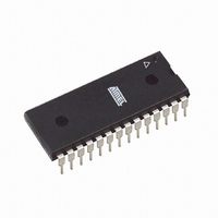
Manufacturer Part Number
ATMEGA168P-20PU
Description
MCU AVR 16K FLASH 20MHZ 28-PDIP
Manufacturer
Atmel
Series
AVR® ATmegar
Specifications of ATMEGA168P-20PU
Core Processor
AVR
Core Size
8-Bit
Speed
20MHz
Connectivity
I²C, SPI, UART/USART
Peripherals
Brown-out Detect/Reset, POR, PWM, WDT
Number Of I /o
23
Program Memory Size
16KB (8K x 16)
Program Memory Type
FLASH
Eeprom Size
512 x 8
Ram Size
1K x 8
Voltage - Supply (vcc/vdd)
2.7 V ~ 5.5 V
Data Converters
A/D 6x10b
Oscillator Type
Internal
Operating Temperature
-40°C ~ 85°C
Package / Case
28-DIP (0.300", 7.62mm)
Processor Series
ATMEGA16x
Core
AVR8
Data Bus Width
8 bit
Data Ram Size
1 KB
Interface Type
I2C, SPI, USART
Maximum Clock Frequency
20 MHz
Number Of Programmable I/os
23
Number Of Timers
3
Maximum Operating Temperature
+ 85 C
Mounting Style
Through Hole
3rd Party Development Tools
EWAVR, EWAVR-BL
Development Tools By Supplier
ATAVRDRAGON, ATSTK500, ATSTK600, ATAVRISP2, ATAVRONEKIT
Minimum Operating Temperature
- 40 C
On-chip Adc
10 bit, 6 Channel
Controller Family/series
AVR MEGA
No. Of I/o's
23
Eeprom Memory Size
512Byte
Ram Memory Size
1KB
Cpu Speed
20MHz
No. Of Timers
3
Rohs Compliant
Yes
Data Rom Size
512 B
A/d Bit Size
10 bit
A/d Channels Available
6
Height
4.57 mm
Length
34.8 mm
Supply Voltage (max)
5.5 V
Supply Voltage (min)
2.7 V
Width
7.49 mm
For Use With
ATSTK600-TQFP32 - STK600 SOCKET/ADAPTER 32-TQFPATAVRDRAGON - KIT DRAGON 32KB FLASH MEM AVR
Lead Free Status / RoHS Status
Lead free / RoHS Compliant
Available stocks
Company
Part Number
Manufacturer
Quantity
Price


23.9
23.9.1
8025L–AVR–7/10
Register Description
ADMUX – ADC Multiplexer Selection Register
• Bit 7:6 – REFS1:0: Reference Selection Bits
These bits select the voltage reference for the ADC, as shown in
changed during a conversion, the change will not go in effect until this conversion is complete
(ADIF in ADCSRA is set). The internal voltage reference options may not be used if an external
reference voltage is being applied to the AREF pin.
Table 23-3.
• Bit 5 – ADLAR: ADC Left Adjust Result
The ADLAR bit affects the presentation of the ADC conversion result in the ADC Data Register.
Write one to ADLAR to left adjust the result. Otherwise, the result is right adjusted. Changing the
ADLAR bit will affect the ADC Data Register immediately, regardless of any ongoing conver-
sions. For a complete description of this bit, see
page
• Bit 4 – Res: Reserved Bit
This bit is an unused bit in the ATmega48P/88P/168P, and will always read as zero.
• Bits 3:0 – MUX3:0: Analog Channel Selection Bits
The value of these bits selects which analog inputs are connected to the ADC. See
for details. If these bits are changed during a conversion, the change will not go in effect until this
conversion is complete (ADIF in ADCSRA is set).
Bit
(0x7C)
Read/Write
Initial Value
REFS1
0
0
1
1
263.
REFS0
REFS1
Voltage Reference Selections for ADC
R/W
0
1
0
1
7
0
REFS0
Voltage Reference Selection
AREF, Internal V
AV
Reserved
Internal 1.1V Voltage Reference with external capacitor at AREF pin
R/W
6
0
CC
with external capacitor at AREF pin
ADLAR
R/W
5
0
ref
turned off
R
4
–
0
MUX3
R/W
”ADCL and ADCH – The ADC Data Register” on
3
0
ATmega48P/88P/168P
MUX2
R/W
2
0
MUX1
R/W
1
0
Table
MUX0
R/W
0
0
23-3. If these bits are
ADMUX
Table 23-4
260
Related parts for ATMEGA168P-20PU
Image
Part Number
Description
Manufacturer
Datasheet
Request
R

Part Number:
Description:
Manufacturer:
Atmel Corporation
Datasheet:
Part Number:
Description:
Manufacturer:
Atmel Corporation
Datasheet:
Part Number:
Description:
Manufacturer:
ATMEL Corporation
Datasheet:

Part Number:
Description:
IC AVR MCU 16K 20MHZ 32TQFP
Manufacturer:
Atmel
Datasheet:

Part Number:
Description:
IC AVR MCU 16K 20MHZ 32-QFN
Manufacturer:
Atmel
Datasheet:

Part Number:
Description:
IC AVR MCU 16K 20MHZ 28DIP
Manufacturer:
Atmel
Datasheet:
Part Number:
Description:
MCU AVR 16K FLASH 15MHZ 32-TQFP
Manufacturer:
Atmel
Datasheet:

Part Number:
Description:
MCU AVR 16K FLASH 15MHZ 32-QFN
Manufacturer:
Atmel
Datasheet:
Part Number:
Description:
IC AVR MCU 16K 20MHZ 32TQFP
Manufacturer:
Atmel
Datasheet:

Part Number:
Description:
MCU AVR 16KB FLASH 20MHZ 32QFN
Manufacturer:
Atmel
Datasheet:
Part Number:
Description:
MCU AVR 16KB FLASH 20MHZ 32TQFP
Manufacturer:
Atmel
Datasheet:

Part Number:
Description:
IC MCU AVR 16K FLASH 32-QFN
Manufacturer:
Atmel
Datasheet: