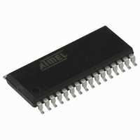
AT90PWM3-16SQ Atmel, AT90PWM3-16SQ Datasheet - Page 217

AT90PWM3-16SQ
Manufacturer Part Number
AT90PWM3-16SQ
Description
IC AVR MCU FLASH 8K 32SOIC
Manufacturer
Atmel
Series
AVR® 90PWM Lightingr
Datasheet
1.AT90PWM3B-16SU.pdf
(361 pages)
Specifications of AT90PWM3-16SQ
Core Processor
AVR
Core Size
8-Bit
Speed
16MHz
Connectivity
SPI, UART/USART
Peripherals
Brown-out Detect/Reset, POR, PWM, WDT
Number Of I /o
27
Program Memory Size
8KB (8K x 8)
Program Memory Type
FLASH
Eeprom Size
512 x 8
Ram Size
512 x 8
Voltage - Supply (vcc/vdd)
2.7 V ~ 5.5 V
Data Converters
A/D 11x10b; D/A 1x10b
Oscillator Type
Internal
Operating Temperature
-40°C ~ 105°C
Package / Case
32-SOIC (7.5mm Width)
Processor Series
AT90PWMx
Core
AVR8
Data Bus Width
8 bit
Data Ram Size
512 B
Interface Type
SPI, USART
Maximum Clock Frequency
16 MHz
Number Of Programmable I/os
27
Number Of Timers
2
Operating Supply Voltage
2.7 V to 5.5 V
Maximum Operating Temperature
+ 105 C
Mounting Style
SMD/SMT
3rd Party Development Tools
EWAVR, EWAVR-BL
Development Tools By Supplier
ATAVRDRAGON, ATSTK500, ATSTK600, ATAVRISP2, ATAVRONEKIT, ATAVRFBKIT, ATAVRISP2
Minimum Operating Temperature
- 40 C
On-chip Adc
10 bit, 11 Channel
On-chip Dac
10 bit, 1 Channel
For Use With
ATSTK600-SOIC - STK600 SOCKET/ADAPTER FOR SOICATAVRMC200 - KIT EVAL FOR AT90PWM3 ASYNCATAVRFBKIT - KIT DEMO BALLAST FOR AT90PWM2ATSTK520 - ADAPTER KIT FOR 90PWM
Lead Free Status / RoHS Status
Lead free / RoHS Compliant
- Current page: 217 of 361
- Download datasheet (7Mb)
19.4
19.4.1
19.4.2
19.4.3
4317J–AVR–08/10
Configuring the EUSART
Data Transmission – EUSART Transmitter
Sending Frames with 5 to 8 Data Bit
Sending Frames with 9, 13, 14, 15 or 16 Data Bit
The EUSART Transmitter is enabled in the same way as standard USART, by setting the Trans-
mit Enable (TXEN) bit in the UCSRB Register. When the Transmitter is enabled, the normal port
operation of the TxDn pin is overridden by the EUSART and given the function as the Transmit-
ter’s serial output. The baud rate, mode of operation and frame format must be set up once
before doing any transmissions. If synchronous operation is used, the clock on the XCK pin will
be overridden and used as transmission clock.
In this mode the behavior is the same as the standard USART (See “Sending Frames with 5 to 8
Data Bit” in USART section).
In these configurations the most significant bits (9, 13, 14, 15 or 16) should be loaded in the
EUDR register before the low byte of the character is written to UDR. The write operation in the
UDR register allows to start the transmission.
Note:
Assembly Code Example
C Code Example
TABLE 2.
EUSART_Transmit:
void EUSART_Transmit( unsigned int data )
{
}
; Wait for empty transmit buffer
sbis UCSRA,UDRE
rjmp EUSART_Transmit
; Put LSB data (r16) and MSN data (r15) into buffer, sends the data
sts
sts
ret
/* Wait for empty transmit buffer */
while ( !( UCSRA & (1<<UDRE))) )
/* Put data into buffer, sends the data */
EUDR = data>>8;
UDR = data;
The example code assumes that the part specific header file is included.
For I/O Registers located in extended I/O map, “IN”, “OUT”, “SBIS”, “SBIC”, “CBI”, and “SBI”
instructions must be replaced with instructions that allow access to extended I/O. Typically “LDS”
and “STS” combined with “SBRS”, “SBRC”, “SBR”, and “CBR”.
EUDR,r15
UDR,r16
(1)
(1)
AT90PWM2/3/2B/3B
217
Related parts for AT90PWM3-16SQ
Image
Part Number
Description
Manufacturer
Datasheet
Request
R

Part Number:
Description:
IC AVR MCU FLASH 8K 32QFN
Manufacturer:
Atmel
Datasheet:

Part Number:
Description:
MCU AVR 8K FLASH 16MHZ 32-QFN
Manufacturer:
Atmel
Datasheet:

Part Number:
Description:
DEV KIT FOR AVR/AVR32
Manufacturer:
Atmel
Datasheet:

Part Number:
Description:
INTERVAL AND WIPE/WASH WIPER CONTROL IC WITH DELAY
Manufacturer:
ATMEL Corporation
Datasheet:

Part Number:
Description:
Low-Voltage Voice-Switched IC for Hands-Free Operation
Manufacturer:
ATMEL Corporation
Datasheet:

Part Number:
Description:
MONOLITHIC INTEGRATED FEATUREPHONE CIRCUIT
Manufacturer:
ATMEL Corporation
Datasheet:

Part Number:
Description:
AM-FM Receiver IC U4255BM-M
Manufacturer:
ATMEL Corporation
Datasheet:

Part Number:
Description:
Monolithic Integrated Feature Phone Circuit
Manufacturer:
ATMEL Corporation
Datasheet:

Part Number:
Description:
Multistandard Video-IF and Quasi Parallel Sound Processing
Manufacturer:
ATMEL Corporation
Datasheet:

Part Number:
Description:
High-performance EE PLD
Manufacturer:
ATMEL Corporation
Datasheet:

Part Number:
Description:
8-bit Flash Microcontroller
Manufacturer:
ATMEL Corporation
Datasheet:

Part Number:
Description:
2-Wire Serial EEPROM
Manufacturer:
ATMEL Corporation
Datasheet:


