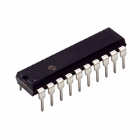
PIC16C770/P Microchip Technology, PIC16C770/P Datasheet - Page 103

PIC16C770/P
Manufacturer Part Number
PIC16C770/P
Description
IC MCU CMOS A/D 2K 20MHZ 20-DIP
Manufacturer
Microchip Technology
Series
PIC® 16Cr
Datasheets
1.PIC16C770-ISO.pdf
(220 pages)
2.PIC16C770-ISO.pdf
(6 pages)
3.PIC16C770-ISO.pdf
(8 pages)
Specifications of PIC16C770/P
Program Memory Type
OTP
Program Memory Size
3.5KB (2K x 14)
Package / Case
20-DIP (0.300", 7.62mm)
Core Processor
PIC
Core Size
8-Bit
Speed
20MHz
Connectivity
I²C, SPI
Peripherals
Brown-out Detect/Reset, POR, PWM, WDT
Number Of I /o
15
Ram Size
256 x 8
Voltage - Supply (vcc/vdd)
4 V ~ 5.5 V
Data Converters
A/D 6x12b
Oscillator Type
Internal
Operating Temperature
0°C ~ 70°C
Processor Series
PIC16C
Core
PIC
Data Bus Width
8 bit
Data Ram Size
256 B
Interface Type
I2C/SPI/SSP
Maximum Clock Frequency
20 MHz
Number Of Programmable I/os
16
Number Of Timers
3
Operating Supply Voltage
2.5 V to 5.5 V
Maximum Operating Temperature
+ 70 C
Mounting Style
Through Hole
3rd Party Development Tools
52715-96, 52716-328, 52717-734
Development Tools By Supplier
ICE2000
Minimum Operating Temperature
0 C
On-chip Adc
6-ch x 12-bit
Lead Free Status / RoHS Status
Lead free / RoHS Compliant
For Use With
DVA16XP200 - ADAPTER ICE 20DIP/SOIC/SSOPAC164028 - MODULE SKT PROMATEII 20SOIC/DIP
Eeprom Size
-
Lead Free Status / Rohs Status
Lead free / RoHS Compliant
- Current page: 103 of 220
- Download datasheet (4Mb)
10.0
The Voltage Reference module provides reference
voltages for the Brown-out Reset circuitry, the Low-volt-
age Detect circuitry and the A/D converter.
REGISTER 10-1: LOW-VOLTAGE DETECT CONTROL REGISTER (LVDCON: 9Ch)
2002 Microchip Technology Inc.
VOLTAGE REFERENCE
MODULE AND LOW-VOLTAGE
DETECT
bit 7-6
bit 5
bit 4
bit 3-0
Unimplemented: Read as '0'
BGST: Bandgap Stable Status Flag bit
1 = Indicates that the bandgap voltage is stable, and LVD interrupt is reliable
0 = Indicates that the bandgap voltage is not stable, and LVD interrupt should not be enabled
LVDEN: Low-voltage Detect Power Enable bit
1 = Enables LVD, powers up bandgap circuit and reference generator
0 = Disables LVD, powers down bandgap circuit if unused by BOR or VRH/VRL
LV<3:0>: Low Voltage Detection Limit bits
1111 = External analog input is used
1110 = 4.5V
1101 = 4.2V
1100 = 4.0V
1011 = 3.8V
1010 = 3.6V
1001 = 3.5V
1000 = 3.3V
0111 = 3.0V
0110 = 2.8V
0101 = 2.7V
0100 = 2.5V
0011 = Reserved. Do not use.
0010 = Reserved. Do not use.
0001 = Reserved. Do not use.
0000 = Reserved. Do not use.
bit 7
Legend:
R = Readable bit
- n = Value at POR
Note:
U-0
—
These are the minimum trip points for the LVD. See Table 15-8 for the trip point tol-
erances. Selection of reserved setting may result in an inadvertent interrupt.
U-0
—
BGST
R-0
W = Writable bit
’1’ = Bit is set
LVDEN
R/W-0
The source for the reference voltages comes from the
bandgap reference circuit. The bandgap circuit is ener-
gized anytime the reference voltage is required by the
other sub-modules, and is powered down when not in
use. The control registers for this module are LVDCON
and REFCON, as shown in Register 10-1 and
Figure 10-2.
(1)
PIC16C717/770/771
R/W-0
U = Unimplemented bit, read as ‘0’
’0’ = Bit is cleared
LV3
R/W-1
LV2
x = Bit is unknown
R/W-0
LV1
DS41120B-page 101
R/W-1
LV0
bit 0
Related parts for PIC16C770/P
Image
Part Number
Description
Manufacturer
Datasheet
Request
R

Part Number:
Description:
IC, 8BIT MCU, PIC16C, 40MHZ, DIP-18
Manufacturer:
Microchip Technology
Datasheet:

Part Number:
Description:
IC, 8BIT MCU, PIC16C, 4MHZ, DIP-28
Manufacturer:
Microchip Technology
Datasheet:

Part Number:
Description:
IC, 8BIT MCU, PIC16C, 4MHZ, DIP-28
Manufacturer:
Microchip Technology
Datasheet:

Part Number:
Description:
IC, 8BIT MCU, PIC16C, 4MHZ, DIP-40
Manufacturer:
Microchip Technology
Datasheet:

Part Number:
Description:
SURFACE MOUNT POWER INDUCTORS
Manufacturer:
RCD [RCD COMPONENTS INC.]
Datasheet:

Part Number:
Description:
Manufacturer:
Microchip Technology Inc.
Datasheet:

Part Number:
Description:
Manufacturer:
Microchip Technology Inc.
Datasheet:

Part Number:
Description:
Manufacturer:
Microchip Technology Inc.
Datasheet:

Part Number:
Description:
Manufacturer:
Microchip Technology Inc.
Datasheet:

Part Number:
Description:
Manufacturer:
Microchip Technology Inc.
Datasheet:

Part Number:
Description:
Manufacturer:
Microchip Technology Inc.
Datasheet:


