AT90PWM1-16SU Atmel, AT90PWM1-16SU Datasheet - Page 222
AT90PWM1-16SU
Manufacturer Part Number
AT90PWM1-16SU
Description
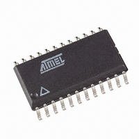
MCU AVR 8K FLASH 16MHZ 24-SOIC
Manufacturer
Atmel
Series
AVR® 90PWM Lightingr
Datasheet
1.AT90PWM1-16SU.pdf
(297 pages)
Specifications of AT90PWM1-16SU
Core Processor
AVR
Core Size
8-Bit
Speed
16MHz
Connectivity
SPI
Peripherals
Brown-out Detect/Reset, POR, PWM, WDT
Number Of I /o
19
Program Memory Size
8KB (8K x 8)
Program Memory Type
FLASH
Eeprom Size
512 x 8
Ram Size
512 x 8
Voltage - Supply (vcc/vdd)
2.7 V ~ 5.5 V
Data Converters
A/D 8x10b
Oscillator Type
Internal
Operating Temperature
-40°C ~ 105°C
Package / Case
24-SOIC (7.5mm Width)
Processor Series
AT90PWMx
Core
AVR8
Data Bus Width
8 bit
Data Ram Size
512 B
Interface Type
SPI
Maximum Clock Frequency
16 MHz
Number Of Programmable I/os
19
Number Of Timers
2
Maximum Operating Temperature
+ 105 C
Mounting Style
SMD/SMT
3rd Party Development Tools
EWAVR, EWAVR-BL
Development Tools By Supplier
ATAVRDRAGON, ATSTK500, ATSTK600, ATAVRISP2, ATAVRONEKIT, ATAVRFBKIT, ATAVRISP2
Minimum Operating Temperature
- 40 C
On-chip Adc
10 bit, 11 Channel
For Use With
ATSTK600-SOIC - STK600 SOCKET/ADAPTER FOR SOIC
Lead Free Status / RoHS Status
Lead free / RoHS Compliant
Available stocks
Company
Part Number
Manufacturer
Quantity
Price

Part Number:
AT90PWM1-16SU
Manufacturer:
ATMEL/爱特梅尔
Quantity:
20 000


22.3.1
222
AT90PWM1
Latching of Fuses
Table 77. Fuse High Byte
Notes:
Table 78. Fuse Low Byte
Note:
The status of the Fuse bits is not affected by Chip Erase. Note that the Fuse bits are locked if
Lock bit1 (LB1) is programmed. Program the Fuse bits before programming the Lock bits.
The fuse values are latched when the device enters programming mode and changes of the
fuse values will have no effect until the part leaves Programming mode. This does not apply to
the EESAVE Fuse which will take effect once it is programmed. The fuses are also latched on
Power-up in Normal mode.
High Fuse Byte
RSTDISBL
DWEN
SPIEN
WDTON
EESAVE
BODLEVEL2
BODLEVEL1
BODLEVEL0
Low Fuse Byte
CKDIV8
CKOUT
SUT1
SUT0
CKSEL3
CKSEL2
CKSEL1
CKSEL0
(2)
1. See
2. The SPIEN Fuse is not accessible in serial programming mode.
3. See
4. See
1. The default value of SUT1..0 results in maximum start-up time for the default clock source.
2. The default setting of CKSEL3..0 results in internal RC Oscillator @ 8 MHz. See
3. The CKOUT Fuse allows the system clock to be output on PORTB0. See
4. See
(3)
(4)
(3)
(1)
See
page 34
Buffer” on page 35
(4)
(4)
(4)
“Alternate Port Functions” on page 63
“Watchdog Timer Configuration” on page 51
Table 9-2 on page 45
Table 7-10 on page 34
“System Clock Prescaler” on page 35
for details.
Bit No
Bit No
for details.
7
6
5
4
3
2
1
0
7
6
5
4
3
2
1
0
for BODLEVEL Fuse decoding.
for details.
Description
External Reset Disable
debugWIRE Enable
Enable Serial Program and
Data Downloading
Watchdog Timer Always On
EEPROM memory is
preserved through the Chip
Erase
Brown-out Detector trigger
level
Brown-out Detector trigger
level
Brown-out Detector trigger
level
Description
Divide clock by 8
Clock output
Select start-up time
Select start-up time
Select Clock source
Select Clock source
Select Clock source
Select Clock source
for details.
for description of RSTDISBL Fuse.
for details.
Default Value
1 (unprogrammed)
1 (unprogrammed)
0 (programmed, SPI
programming enabled)
1 (unprogrammed)
1 (unprogrammed), EEPROM
not reserved
1 (unprogrammed)
1 (unprogrammed)
1 (unprogrammed)
Default Value
0 (programmed)
1 (unprogrammed)
1 (unprogrammed)
0 (programmed)
0 (programmed)
0 (programmed)
1 (unprogrammed)
0 (programmed)
4378C–AVR–09/08
(1)
(2)
(2)
(2)
“Clock Output
Table 7-10 on
(1)
(2)
Related parts for AT90PWM1-16SU
Image
Part Number
Description
Manufacturer
Datasheet
Request
R

Part Number:
Description:
Manufacturer:
Atmel Corporation
Datasheet:

Part Number:
Description:
IC AVR PWM 8KB FLASH 16MHZ 32QFN
Manufacturer:
Atmel
Datasheet:

Part Number:
Description:
DEV KIT FOR AVR/AVR32
Manufacturer:
Atmel
Datasheet:
Part Number:
Description:
INTERVAL AND WIPE/WASH WIPER CONTROL IC WITH DELAY
Manufacturer:
ATMEL Corporation
Datasheet:
Part Number:
Description:
Low-Voltage Voice-Switched IC for Hands-Free Operation
Manufacturer:
ATMEL Corporation
Datasheet:
Part Number:
Description:
MONOLITHIC INTEGRATED FEATUREPHONE CIRCUIT
Manufacturer:
ATMEL Corporation
Datasheet:
Part Number:
Description:
AM-FM Receiver IC U4255BM-M
Manufacturer:
ATMEL Corporation
Datasheet:
Part Number:
Description:
Monolithic Integrated Feature Phone Circuit
Manufacturer:
ATMEL Corporation
Datasheet:
Part Number:
Description:
Multistandard Video-IF and Quasi Parallel Sound Processing
Manufacturer:
ATMEL Corporation
Datasheet:
Part Number:
Description:
High-performance EE PLD
Manufacturer:
ATMEL Corporation
Datasheet:
Part Number:
Description:
8-bit Flash Microcontroller
Manufacturer:
ATMEL Corporation
Datasheet: