ATMEGA48PA-PU Atmel, ATMEGA48PA-PU Datasheet - Page 178
ATMEGA48PA-PU
Manufacturer Part Number
ATMEGA48PA-PU
Description
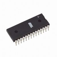
MCU AVR 4KB FLASH IND 28PDIP
Manufacturer
Atmel
Series
AVR® ATmegar
Specifications of ATMEGA48PA-PU
Core Processor
AVR
Core Size
8-Bit
Speed
20MHz
Connectivity
I²C, SPI, UART/USART
Peripherals
Brown-out Detect/Reset, POR, PWM, WDT
Number Of I /o
23
Program Memory Size
4KB (2K x 16)
Program Memory Type
FLASH
Eeprom Size
256 x 8
Ram Size
512 x 8
Voltage - Supply (vcc/vdd)
1.8 V ~ 5.5 V
Data Converters
A/D 6x10b
Oscillator Type
Internal
Operating Temperature
-40°C ~ 85°C
Package / Case
28-DIP (0.300", 7.62mm)
Processor Series
ATMEGA48x
Core
AVR8
Data Bus Width
8 bit
Data Ram Size
512 B
Interface Type
2-Wire, SPI, USART
Maximum Clock Frequency
20 MHz
Number Of Programmable I/os
23
Number Of Timers
3
Maximum Operating Temperature
+ 85 C
Mounting Style
Through Hole
3rd Party Development Tools
EWAVR, EWAVR-BL
Development Tools By Supplier
ATAVRDRAGON, ATSTK500, ATSTK600, ATAVRISP2, ATAVRONEKIT
Minimum Operating Temperature
- 40 C
On-chip Adc
10 bit, 6 Channel
On-chip Dac
10 bit, 6 Channel
For Use With
ATSTK600 - DEV KIT FOR AVR/AVR32ATAVRDRAGON - KIT DRAGON 32KB FLASH MEM AVR
Lead Free Status / RoHS Status
Lead free / RoHS Compliant
Available stocks
Company
Part Number
Manufacturer
Quantity
Price
Company:

Part Number:
ATMEGA48PA-PU
Manufacturer:
ON
Quantity:
21 000


19.3
8271C–AVR–08/10
Clock Generation
Figure 19-1. USART Block Diagram
Note:
The Clock Generation logic generates the base clock for the Transmitter and Receiver. The
USART supports four modes of clock operation: Normal asynchronous, Double Speed asyn-
chronous, Master synchronous and Slave synchronous mode. The UMSELn bit in USART
Control and Status Register C (UCSRnC) selects between asynchronous and synchronous
operation. Double Speed (asynchronous mode only) is controlled by the U2Xn found in the
UCSRnA Register. When using synchronous mode (UMSELn = 1), the Data Direction Register
for the XCKn pin (DDR_XCKn) controls whether the clock source is internal (Master mode) or
external (Slave mode). The XCKn pin is only active when using synchronous mode.
ATmega48A/48PA/88A/88PA/168A/168PA/328/328
1. Refer to
Figure 1-1 on page 2
UCSRnA
TRANSMIT SHIFT REGISTER
RECEIVE SHIFT REGISTER
BAUD RATE GENERATOR
UDRn (Receive)
UDRn(Transmit)
UBRRn [H:L]
(1)
and
Table 13-9 on page 89
UCSRnB
GENERATOR
SYNC LOGIC
RECOVERY
RECOVERY
CHECKER
PARITY
PARITY
CLOCK
DATA
OSC
for USART0 pin placement.
Clock Generator
CONTROL
CONTROL
CONTROL
CONTROL
CONTROL
Transmitter
PIN
PIN
PIN
RX
TX
Receiver
UCSRnC
XCKn
TxDn
RxDn
178
Related parts for ATMEGA48PA-PU
Image
Part Number
Description
Manufacturer
Datasheet
Request
R

Part Number:
Description:
IC AVR MCU 4K 5V 20MHZ 32-TQFP
Manufacturer:
Atmel
Datasheet:

Part Number:
Description:
Manufacturer:
Atmel Corporation
Datasheet:
Part Number:
Description:
Manufacturer:
Atmel Corporation
Datasheet:
Part Number:
Description:
IC AVR MCU 4K 20MHZ 5V 32TQFP
Manufacturer:
Atmel
Datasheet:

Part Number:
Description:
IC AVR MCU 4K 20MHZ 5V 28DIP
Manufacturer:
Atmel
Datasheet:

Part Number:
Description:
IC AVR MCU 4K 20MHZ 5V 32-QFN
Manufacturer:
Atmel
Datasheet:

Part Number:
Description:
IC AVR MCU 4K 5V 20MHZ 32-TQFP
Manufacturer:
Atmel
Datasheet:

Part Number:
Description:
IC AVR MCU 4K 5V 20MHZ 32-QFN
Manufacturer:
Atmel
Datasheet:
Part Number:
Description:
IC AVR MCU 4K 5V 20MHZ 32-QFN
Manufacturer:
Atmel
Datasheet:
Part Number:
Description:
IC AVR MCU 4K 5V 20MHZ 28-DIP
Manufacturer:
Atmel
Datasheet:
Part Number:
Description:
IC AVR MCU 4K 5V 20MHZ 28-DIP
Manufacturer:
Atmel
Datasheet:

Part Number:
Description:
IC AVR MCU 4K FLASH 20MHZ 28QFN
Manufacturer:
Atmel
Datasheet: