PIC16F785-E/P Microchip Technology, PIC16F785-E/P Datasheet - Page 7
PIC16F785-E/P
Manufacturer Part Number
PIC16F785-E/P
Description
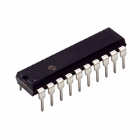
IC PIC MCU FLASH 2KX14 20DIP
Manufacturer
Microchip Technology
Series
PIC® 16Fr
Datasheets
1.PIC16F616T-ISL.pdf
(8 pages)
2.PIC16F785-ISS.pdf
(206 pages)
3.PIC16F785-ISS.pdf
(10 pages)
4.PIC16F785-ISS.pdf
(28 pages)
Specifications of PIC16F785-E/P
Core Processor
PIC
Core Size
8-Bit
Speed
20MHz
Peripherals
Brown-out Detect/Reset, POR, PWM, WDT
Number Of I /o
17
Program Memory Size
3.5KB (2K x 14)
Program Memory Type
FLASH
Eeprom Size
256 x 8
Ram Size
128 x 8
Voltage - Supply (vcc/vdd)
2 V ~ 5.5 V
Data Converters
A/D 14x10b
Oscillator Type
Internal
Operating Temperature
-40°C ~ 125°C
Package / Case
20-DIP (0.300", 7.62mm)
For Use With
AC162060 - HEADER INTRFC MPLAB ICD2 20PINAC164039 - MODULE SKT PROMATE II 20DIP/SOICDM163029 - BOARD PICDEM FOR MECHATRONICSACICE0203 - MPLABICE 20P 300 MIL ADAPTER
Lead Free Status / RoHS Status
Lead free / RoHS Compliant
Connectivity
-


3.1
The PIC16F785/HV785 program memory may be
written in two ways. The fastest method writes four
words at a time. However, one-word writes are also
supported for backward compatibility with previous 8-
pin and 14-pin Flash devices. The four-word algorithm
is used to program the program memory and the user
ID locations only. The one-word algorithm can write any
available memory location (i.e., program memory,
configuration memory and data memory).
After writing the array, the PC may be reset and the
entire array read back to verify the write. It is not
possible to verify immediately following the write
because the PC can only increment, not decrement.
A device Reset will clear the PC and set the address to
‘0’. The Increment Address command will increment
the PC. The Load Configuration command will set the
PC to 0x2000. The available commands are shown in
Table 3-1.
3.1.1
Only the program memory can be written using this
algorithm. Data and configuration memory (>0x2003)
must use the one-word programming algorithm
(Section 3.1.2 “One-Word Programming”).
This algorithm writes four sequential addresses in
program memory. The four addresses must point to a
four-word block with addresses modulo 4 of 0, 1, 2 and
3. For example, programming address 4 through 7 can
be programmed together. Programming addresses 2
through 5 will create an unexpected result.
The sequence for programming four words of program
memory at a time is as follows:
1.
2.
3.
4.
5.
6.
7.
8.
9.
See Figure 3-17 for more information.
2009 Microchip Technology Inc.
Load a word at the current program memory
address using Load Data for Program Memory
command.
Issue an Increment Address command.
Load a word at the current program memory
address using Load Data for Program Memory
command.
Repeat Steps 2 and 3, two more times.
Issue a Begin Programming command, either
internally or externally timed.
Wait T
(externally timed).
Issue an End Programming command if externally
timed.
Issue an Increment Address command.
Repeat steps 1 through 8 as required to write
program memory.
Program/Erase Algorithms
FOUR-WORD PROGRAMMING
PROG
1 (internally timed) or T
PROG
2
3.1.2
The program memory may also be written one-word at
a time to allow compatibility with other 8-pin and 14-pin
Flash PIC
and data memory must be written one-word (or byte) at
a time with the exception of the user ID locations.
The sequence for programming one-word of program
memory at a time is as follows:
1.
2.
3.
4.
5.
6.
See Figure 3-16 for more information.
3.1.3
The user ID (0x2000-0x2003) and Configuration Word
(0x2007) are mapped into the configuration memory
but do not physically reside in it. As a result, the write
latches are not reset when programming these
locations and must be reset by the programmer. This
can be done in two ways, either loading all four latches
with ‘1’s or by exiting Program/Verify mode.
The sequence for manually resetting the write latches
is as follows:
1.
2.
3.
Note:
Load a word at the current program memory
address using Load Data for Program Memory
command.
Issue a Begin Programming command either
internally or externally timed.
Wait T
(externally timed).
Issue an End Programming command if
externally timed.
Issue an Increment Address command.
Repeat this sequence as required to write
program, data or configuration memory.
Load a word using Load Data for Program
Memory command with a data word of all ‘1’s.
Issue an Increment Address command.
Repeat this sequence three times to all four
write latches to 1’s (Reset state).
PIC16F785/HV785
®
ONE-WORD PROGRAMMING
The four write latches must be reset after
programming
0x2003) or Configuration Word (0x2007).
See Section 3.1.3 “Resetting Write
Latches”.
RESETTING WRITE LATCHES
devices. Configuration memory (>0x2003)
PROG
1 (internally timed) or T
the
user
DS41237D-page 7
ID
(0x2000-
PROG
2
Related parts for PIC16F785-E/P
Image
Part Number
Description
Manufacturer
Datasheet
Request
R

Part Number:
Description:
3.5KB Flash, 128B RAM, 18 I/O, CLC, CWG, DDS, 10-bit ADC 20 QFN 4x4mm TUBE
Manufacturer:
Microchip Technology
Datasheet:

Part Number:
Description:
3.5KB Flash, 128B RAM, 18 I/O, CLC, CWG, DDS, 10-bit ADC 20 PDIP .300in TUBE
Manufacturer:
Microchip Technology
Datasheet:

Part Number:
Description:
3.5KB Flash, 128B RAM, 18 I/O, CLC, CWG, DDS, 10-bit ADC 20 SOIC .300in TUBE
Manufacturer:
Microchip Technology
Datasheet:

Part Number:
Description:
3.5KB Flash, 128B RAM, 18 I/O, CLC, CWG, DDS, 10-bit ADC 20 SSOP .209in TUBE
Manufacturer:
Microchip Technology
Datasheet:
Part Number:
Description:
3.5KB Flash, 128B RAM, 18 I/O, CLC, CWG, DDS, 10-bit ADC 20 QFN 4x4mm TUBE
Manufacturer:
Microchip Technology
Datasheet:
Part Number:
Description:
3.5KB Flash, 128B RAM, 18 I/O, CLC, CWG, DDS, 10-bit ADC 20 PDIP .300in TUBE
Manufacturer:
Microchip Technology
Datasheet:
Part Number:
Description:
3.5KB Flash, 128B RAM, 18 I/O, CLC, CWG, DDS, 10-bit ADC 20 SOIC .300in TUBE
Manufacturer:
Microchip Technology
Datasheet:
Part Number:
Description:
3.5KB Flash, 128B RAM, 18 I/O, CLC, CWG, DDS, 10-bit ADC 20 SSOP .209in TUBE
Manufacturer:
Microchip Technology
Datasheet:
Part Number:
Description:
3.5KB Flash, 128B RAM, 18 I/O, CLC, CWG, DDS, 10-bit ADC 20 QFN 4x4mm T/R
Manufacturer:
Microchip Technology
Datasheet:
Part Number:
Description:
3.5KB Flash, 128B RAM, 18 I/O, CLC, CWG, DDS, 10-bit ADC 20 SOIC .300in T/R
Manufacturer:
Microchip Technology
Datasheet:
Part Number:
Description:
3.5KB Flash, 128B RAM, 18 I/O, CLC, CWG, DDS, 10-bit ADC 20 SSOP .209in T/R
Manufacturer:
Microchip Technology
Datasheet:
Part Number:
Description:
3.5KB Flash, 128B RAM, 18 I/O, CLC, CWG, DDS, 10-bit ADC 20 QFN 4x4mm TUBE
Manufacturer:
Microchip Technology
Datasheet:
Part Number:
Description:
3.5KB Flash, 128B RAM, 18 I/O, CLC, CWG, DDS, 10-bit ADC 20 PDIP .300in TUBE
Manufacturer:
Microchip Technology
Datasheet:
Part Number:
Description:
3.5KB Flash, 128B RAM, 18 I/O, CLC, CWG, DDS, 10-bit ADC 20 SOIC .300in TUBE
Manufacturer:
Microchip Technology
Datasheet:
Part Number:
Description:
3.5KB Flash, 128B RAM, 18 I/O, CLC, CWG, DDS, 10-bit ADC 20 SSOP .209in TUBE
Manufacturer:
Microchip Technology
Datasheet: