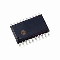
PIC16F685-E/SO Microchip Technology, PIC16F685-E/SO Datasheet - Page 193

PIC16F685-E/SO
Manufacturer Part Number
PIC16F685-E/SO
Description
IC PIC MCU FLASH 4KX14 20SOIC
Manufacturer
Microchip Technology
Series
PIC® 16Fr
Datasheets
1.PIC16F616T-ISL.pdf
(8 pages)
2.PIC16F690DM-PCTLHS.pdf
(306 pages)
3.PIC16F677-IP.pdf
(2 pages)
4.PIC16F677-IP.pdf
(16 pages)
Specifications of PIC16F685-E/SO
Core Processor
PIC
Core Size
8-Bit
Speed
20MHz
Peripherals
Brown-out Detect/Reset, POR, PWM, WDT
Number Of I /o
18
Program Memory Size
7KB (4K x 14)
Program Memory Type
FLASH
Eeprom Size
256 x 8
Ram Size
256 x 8
Voltage - Supply (vcc/vdd)
2 V ~ 5.5 V
Data Converters
A/D 12x10b
Oscillator Type
Internal
Operating Temperature
-40°C ~ 125°C
Package / Case
20-SOIC (7.5mm Width)
For Use With
XLT20SO1-1 - SOCKET TRANS ICE 20DIP TO 20SOICAC162061 - HEADER INTRFC MPLAB ICD2 20PINAC164039 - MODULE SKT PROMATE II 20DIP/SOIC
Lead Free Status / RoHS Status
Lead free / RoHS Compliant
Connectivity
-
- PIC16F616T-ISL PDF datasheet
- PIC16F690DM-PCTLHS PDF datasheet #2
- PIC16F677-IP PDF datasheet #3
- PIC16F677-IP PDF datasheet #4
- Current page: 193 of 306
- Download datasheet (6Mb)
13.12.3
An SSP Mask (SSPMSK) register is available in I
Slave mode as a mask for the value held in the
SSPSR register during an address comparison
operation. A zero (‘0’) bit in the SSPMSK register has
the effect of making the corresponding bit in the
SSPSR register a ‘don’t care’.
This register is reset to all ‘1’s upon any Reset
condition and, therefore, has no effect on standard
SSP operation until written with a mask value.
REGISTER 13-3:
© 2008 Microchip Technology Inc.
bit 7
Legend:
R = Readable bit
-n = Value at POR
bit 7-1
bit 0
Note 1: When SSPCON bits SSPM<3:0> = 1001, any reads or writes to the SSPADD SFR address are accessed
R/W-1
MSK7
2: In all other SSP modes, this bit has no effect.
SSP MASK REGISTER
through the SSPMSK register. The SSPEN bit of the SSPCON register should be zero when accessing
the SSPMSK register.
MSK<7:1>: Mask bits
1 = The received address bit n is compared to SSPADD<n> to detect I
0 = The received address bit n is not used to detect I
MSK<0>: Mask bit for I
I
1 = The received address bit 0 is compared to SSPADD<0> to detect I
0 = The received address bit 0 is not used to detect I
2
C Slave mode, 10-bit Address (SSPM<3:0> = 0111):
R/W-1
MSK6
SSPMSK: SSP MASK REGISTER
W = Writable bit
‘1’ = Bit is set
R/W-1
MSK5
PIC16F631/677/685/687/689/690
2
C Slave mode, 10-bit Address
R/W-1
MSK4
2
C
U = Unimplemented bit, read as ‘0’
‘0’ = Bit is cleared
(1)
R/W-1
MSK3
This register must be initiated prior to setting
SSPM<3:0> bits to select the I
10-bit address).
This register can only be accessed when the appropriate
mode is selected by bits (SSPM<3:0> of SSPCON).
The SSP Mask register is active during:
• 7-bit Address mode: address compare of A<7:1>.
• 10-bit Address mode: address compare of A<7:0>
only. The SSP mask has no effect during the
reception of the first (high) byte of the address.
2
2
C address match
(2)
C address match
R/W-1
MSK2
2
2
C address match
C address match
x = Bit is unknown
R/W-1
MSK1
2
C Slave mode (7-bit or
DS41262E-page 191
MSK0
R/W-1
(2)
bit 0
Related parts for PIC16F685-E/SO
Image
Part Number
Description
Manufacturer
Datasheet
Request
R

Part Number:
Description:
IC PIC MCU FLASH 4KX14 20SSOP
Manufacturer:
Microchip Technology
Datasheet:

Part Number:
Description:
IC PIC MCU FLASH 4KX14 20DIP
Manufacturer:
Microchip Technology
Datasheet:

Part Number:
Description:
IC PIC MCU FLASH 4KX14 20SOIC
Manufacturer:
Microchip Technology
Datasheet:

Part Number:
Description:
IC,MICROCONTROLLER,8-BIT,PIC CPU,CMOS,LLCC,20PIN,PLASTIC
Manufacturer:
Microchip Technology
Datasheet:

Part Number:
Description:
IC PIC MCU FLASH 4KX14 20SSOP
Manufacturer:
Microchip Technology
Datasheet:

Part Number:
Description:
IC PIC MCU FLASH 4KX14 20DIP
Manufacturer:
Microchip Technology
Datasheet:

Part Number:
Description:
IC,MICROCONTROLLER,8-BIT,PIC CPU,CMOS,LLCC,20PIN,PLASTIC
Manufacturer:
Microchip Technology
Datasheet:

Part Number:
Description:
IC, 8BIT MCU, PIC16F, 32MHZ, SOIC-18
Manufacturer:
Microchip Technology
Datasheet:

Part Number:
Description:
IC, 8BIT MCU, PIC16F, 32MHZ, SSOP-20
Manufacturer:
Microchip Technology
Datasheet:

Part Number:
Description:
IC, 8BIT MCU, PIC16F, 32MHZ, DIP-18
Manufacturer:
Microchip Technology
Datasheet:

Part Number:
Description:
IC, 8BIT MCU, PIC16F, 32MHZ, QFN-28
Manufacturer:
Microchip Technology
Datasheet:

Part Number:
Description:
IC, 8BIT MCU, PIC16F, 32MHZ, QFN-28
Manufacturer:
Microchip Technology
Datasheet:

Part Number:
Description:
IC, 8BIT MCU, PIC16F, 32MHZ, QFN-28
Manufacturer:
Microchip Technology
Datasheet:

Part Number:
Description:
IC, 8BIT MCU, PIC16F, 32MHZ, SSOP-20
Manufacturer:
Microchip Technology
Datasheet:

Part Number:
Description:
IC, 8BIT MCU, PIC16F, 20MHZ, DIP-40
Manufacturer:
Microchip Technology
Datasheet:


