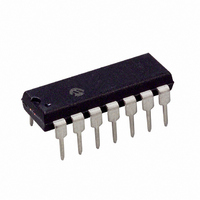
PIC16F684-E/P Microchip Technology, PIC16F684-E/P Datasheet - Page 83

PIC16F684-E/P
Manufacturer Part Number
PIC16F684-E/P
Description
IC PIC MCU FLASH 2KX14 14DIP
Manufacturer
Microchip Technology
Series
PIC® 16Fr
Datasheets
1.PIC16F616T-ISL.pdf
(8 pages)
2.PIC16F688T-ISL.pdf
(688 pages)
3.PIC16F684-ISL.pdf
(4 pages)
4.PIC16F684-ISL.pdf
(192 pages)
5.PIC16F684-ISL.pdf
(6 pages)
6.PIC16F684-IST.pdf
(164 pages)
Specifications of PIC16F684-E/P
Program Memory Type
FLASH
Program Memory Size
3.5KB (2K x 14)
Package / Case
14-DIP (0.300", 7.62mm)
Core Processor
PIC
Core Size
8-Bit
Speed
20MHz
Peripherals
Brown-out Detect/Reset, POR, PWM, WDT
Number Of I /o
12
Eeprom Size
256 x 8
Ram Size
128 x 8
Voltage - Supply (vcc/vdd)
2 V ~ 5.5 V
Data Converters
A/D 8x10b
Oscillator Type
Internal
Operating Temperature
-40°C ~ 125°C
Processor Series
PIC16F
Core
PIC
Data Bus Width
8 bit
Data Ram Size
128 B
Maximum Clock Frequency
20 MHz
Number Of Programmable I/os
12
Number Of Timers
3
Operating Supply Voltage
2 V to 5.5 V
Maximum Operating Temperature
+ 125 C
Mounting Style
Through Hole
3rd Party Development Tools
52715-96, 52716-328, 52717-734
Development Tools By Supplier
PG164130, DV164035, DV244005, DV164005, PG164120, ICE2000, DM163014, DM164120-4
Minimum Operating Temperature
- 40 C
On-chip Adc
8-ch x 10-bit
Lead Free Status / RoHS Status
Lead free / RoHS Compliant
For Use With
DM163029 - BOARD PICDEM FOR MECHATRONICSACICE0207 - MPLABICE 14P 300 MIL ADAPTER
Connectivity
-
Lead Free Status / Rohs Status
Lead free / RoHS Compliant
11.3.4
In the Half-bridge Output mode, two pins are used as
outputs to drive push-pull loads. The PWM output sig-
nal is output on the RC5/CCP1/P1A pin, while the com-
plementary PWM output signal is output on the
RC4/C2OUT/P1B pin (Figure 11-6). This mode can be
used for half-bridge applications, as shown in
Figure 11-7, or for full-bridge applications, where four
power switches are being modulated with two PWM
signals.
In Half-bridge Output mode, the programmable dead
band delay can be used to prevent shoot-through
current in half-bridge power devices. The value of bits
PDC<6:0> (PWM1CON<6:0>) sets the number of
instruction cycles before the output is driven active. If
the value is greater than the duty cycle, the corre-
sponding output remains inactive during the entire
cycle. See Section 11.3.6 “Programmable Dead
Band Delay” for more details of the dead band delay
operations.
FIGURE 11-7:
2004 Microchip Technology Inc.
Standard Half-bridge Circuit (“Push-Pull”)
Half-bridge Output Driving a Full-bridge Circuit
HALF-BRIDGE MODE
PIC16F684
EXAMPLES OF HALF-BRIDGE APPLICATIONS
P1A
P1B
PIC16F684
P1A
P1B
FET
Driver
FET
Driver
Preliminary
FET
Driver
FET
Driver
Since the P1A and P1B outputs are multiplexed with
the PORTC<5:4> data latches, the TRISC<5:4> bits
must be cleared to configure P1A and P1B as outputs.
FIGURE 11-6:
P1A
P1B
td = Dead Band Delay
Load
Note 1: At this time, the TMR2 register is equal to the
V+
V-
(2)
(2)
V+
V-
2: Output signals are shown as active-high.
(1)
td
Duty Cycle
PR2 register.
Load
Period
td
FET
Driver
FET
Driver
HALF-BRIDGE PWM
OUTPUT
+
V
-
+
V
-
PIC16F684
(1)
Period
DS41202C-page 81
(1)


