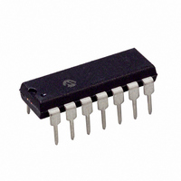
PIC16F684-E/P Microchip Technology, PIC16F684-E/P Datasheet - Page 80

PIC16F684-E/P
Manufacturer Part Number
PIC16F684-E/P
Description
IC PIC MCU FLASH 2KX14 14DIP
Manufacturer
Microchip Technology
Series
PIC® 16Fr
Datasheets
1.PIC16F616T-ISL.pdf
(8 pages)
2.PIC16F688T-ISL.pdf
(688 pages)
3.PIC16F684-ISL.pdf
(4 pages)
4.PIC16F684-ISL.pdf
(192 pages)
5.PIC16F684-ISL.pdf
(6 pages)
6.PIC16F684-IST.pdf
(164 pages)
Specifications of PIC16F684-E/P
Program Memory Type
FLASH
Program Memory Size
3.5KB (2K x 14)
Package / Case
14-DIP (0.300", 7.62mm)
Core Processor
PIC
Core Size
8-Bit
Speed
20MHz
Peripherals
Brown-out Detect/Reset, POR, PWM, WDT
Number Of I /o
12
Eeprom Size
256 x 8
Ram Size
128 x 8
Voltage - Supply (vcc/vdd)
2 V ~ 5.5 V
Data Converters
A/D 8x10b
Oscillator Type
Internal
Operating Temperature
-40°C ~ 125°C
Processor Series
PIC16F
Core
PIC
Data Bus Width
8 bit
Data Ram Size
128 B
Maximum Clock Frequency
20 MHz
Number Of Programmable I/os
12
Number Of Timers
3
Operating Supply Voltage
2 V to 5.5 V
Maximum Operating Temperature
+ 125 C
Mounting Style
Through Hole
3rd Party Development Tools
52715-96, 52716-328, 52717-734
Development Tools By Supplier
PG164130, DV164035, DV244005, DV164005, PG164120, ICE2000, DM163014, DM164120-4
Minimum Operating Temperature
- 40 C
On-chip Adc
8-ch x 10-bit
Lead Free Status / RoHS Status
Lead free / RoHS Compliant
For Use With
DM163029 - BOARD PICDEM FOR MECHATRONICSACICE0207 - MPLABICE 14P 300 MIL ADAPTER
Connectivity
-
Lead Free Status / Rohs Status
Lead free / RoHS Compliant
PIC16F684
11.3
The Enhanced CCP module produces up to a 10-bit
resolution PWM output and may have up to four
outputs, depending on the selected operating mode.
These outputs, designated P1A through P1D, are
multiplexed with I/O pins on PORTC. The pin
assignments are summarized in Table 11-3.
FIGURE 11-3:
11.3.1
The P1M<1:0> bits in the CCP1CON register allows
one of four configurations:
• Single Output
• Half-bridge Output
• Full-bridge Output, Forward mode
• Full-bridge Output, Reverse mode
TABLE 11-3:
DS41202C-page 78
Compatible CCP
Dual PWM
Quad PWM
Legend: x = Don’t care. Shaded cells indicate pin assignments not used by ECCP in a given mode.
Note 1:
CCPR1H (Slave)
Duty Cycle Registers
Note 1: The 8-bit timer TMR2 register is concatenated with the 2-bit internal Q clock, or 2 bits of the prescaler to
Comparator
2:
Enhanced PWM Mode
CCPR1L
PR2
TMR2
Comparator
ECCP Mode
TRIS register values must be configured appropriately.
With ECCP in Dual or Quad PWM mode, the C2OUT output control of PORTC must be disabled.
PWM OUTPUT CONFIGURATIONS
create the 10-bit time base.
PIN ASSIGNMENTS FOR VARIOUS ENHANCED CCP MODES
(1)
SIMPLIFIED BLOCK DIAGRAM OF THE ENHANCED PWM MODULE
Clear Timer2,
toggle PWM pin and
latch duty cycle
CCP1CON<5:4>
Configuration
R
S
CCP1CON
00xx11xx
10xx11xx
x1xx11xx
P1M<1:0>
Q
Preliminary
PWM1CON
Controller
Output
2
CCP1/P1A
CCP1
RC5
P1A
P1A
P1C
P1D
P1B
Figure 11-3 shows a simplified block diagram of PWM
operation.
To configure I/O pins as PWM outputs, the proper PWM
mode must be selected by setting the P1M<1:0> and
CCP1M<3:0>
CCP1CON<3:0>,
TRISC bits must also be set as outputs.
The general relationship of the outputs in all
configurations is summarized in Figure 11-3.
4
CCP1M<3:0>
Note:
RC4/C2OUT
TRISC<5>
TRISC<4>
TRISC<3>
TRISC<2>
Clearing the CCP1CON register will force
the PWM output latches to their default
inactive levels. This is not the PORTC I/O
data latch.
RC4
P1B
P1B
bits
respectively).
2004 Microchip Technology Inc.
RC3/AN7
RC3/AN7
(CCP1CON<7:6>
RC3
P1C
RC5/CCP1/P1A
RC4/C2OUT/P1B
RC3/AN7/P1C
RC2/AN6/P1D
The
RC2/AN6
RC2/AN6
appropriate
RC2
P1D
and


